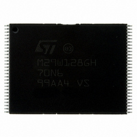
M29W128GH70N6E NUMONYX, M29W128GH70N6E Datasheet - Page 35

M29W128GH70N6E
Manufacturer Part Number
M29W128GH70N6E
Description
IC FLASH 128MBIT 70NS 56TSOP
Manufacturer
NUMONYX
Series
Axcell™r
Datasheet
1.M29W128GH70N6E.pdf
(94 pages)
Specifications of M29W128GH70N6E
Format - Memory
FLASH
Memory Type
FLASH
Memory Size
128M (16Mx8, 8Mx16)
Speed
70ns
Interface
Parallel
Voltage - Supply
2.7 V ~ 3.6 V
Operating Temperature
-40°C ~ 85°C
Package / Case
56-TSOP
Package
56TSOP
Cell Type
NOR
Density
128 Mb
Architecture
Sectored
Block Organization
Symmetrical
Typical Operating Supply Voltage
3|3.3 V
Sector Size
128KByte x 128
Timing Type
Asynchronous
Interface Type
Parallel
Lead Free Status / RoHS Status
Lead free / RoHS Compliant
Available stocks
Company
Part Number
Manufacturer
Quantity
Price
Company:
Part Number:
M29W128GH70N6E
Manufacturer:
Numonyx
Quantity:
17 280
Company:
Part Number:
M29W128GH70N6E
Manufacturer:
MICRON
Quantity:
595
Company:
Part Number:
M29W128GH70N6E
Manufacturer:
MICRON45
Quantity:
556
Part Number:
M29W128GH70N6E
Manufacturer:
ST
Quantity:
20 000
6.2.2
All the addresses used in the write to buffer program operation must lie within the same
page.
To program the content of the write buffer, this command must be followed by a Write to
Buffer Program Confirm command.
If an address is written several times during a write to buffer program operation, the
address/data counter will be decremented at each data load operation and the data will be
programmed to the last word loaded into the buffer.
Invalid address combinations or failing to follow the correct sequence of bus write cycles will
abort the write to buffer program.
The status register bits DQ1, DQ5, DQ6, DQ7 can be used to monitor the device status
during a write to buffer program operation.
It is possible to detect program operation fails when changing programmed data from ‘0’ to
‘1’, that is when reprogramming data in a portion of memory already programmed.
See
suggested flowchart on using the Write to Buffer Program command.
Enhanced Buffered Program command
The Enhanced Buffered Program command, available only in x 16 mode, makes use of the
device’s 256-word write buffer to speed up programming. 256 words can be loaded into the
write buffer. Each write buffer has the same A22-A8 addresses. The Enhanced Buffered
Program command dramatically reduces system programming time compared to both the
standard non-buffered Program command and the Write to Buffer command.
When issuing an Enhanced Buffered Program command, the V
High, V
See
typical enhanced buffered program times in both cases.
Three successive steps are required to issue the Enhanced Buffered Program command:
To program the content of the write buffer, the Enhanced Buffered Program command must
be followed by an Enhanced Buffered Program Confirm command. The command ends with
an internal enhanced buffered program confirm cycle.
Note that address/data cycles must be loaded in an increasing address order (from
ADD[7:0]=00000000 to ADD[7:0]=11111111) and completely (all 256 words). Invalid address
combinations or failing to follow the correct sequence of bus write cycles will abort the
enhanced buffered program.
The status register bits DQ1, DQ5, DQ6, and DQ7 can be used to monitor the device status
during an enhanced buffered program operation.
An external supply (12 V) can be used to improve programming efficiency.
Appendix
Table 17: Program, erase times and program, erase endurance cycles
The Enhanced Buffered Program command starts with two unlock cycles
The third bus write cycle sets up the Enhanced Buffered Program command. The setup
code can be addressed to any location within the targeted block
The fourth bus write cycle loads the first address and data to be programmed. There a
total of 256 address and data loading cycles.
IH
, or raised to V
D,
Figure 30: Write to buffer program flowchart and
PPH
.
PP
/WP pin can be either held
pseudocode, for a
for details on
35/94


