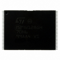
M29W128GH70N6E NUMONYX, M29W128GH70N6E Datasheet - Page 15

M29W128GH70N6E
Manufacturer Part Number
M29W128GH70N6E
Description
IC FLASH 128MBIT 70NS 56TSOP
Manufacturer
NUMONYX
Series
Axcell™r
Datasheet
1.M29W128GH70N6E.pdf
(94 pages)
Specifications of M29W128GH70N6E
Format - Memory
FLASH
Memory Type
FLASH
Memory Size
128M (16Mx8, 8Mx16)
Speed
70ns
Interface
Parallel
Voltage - Supply
2.7 V ~ 3.6 V
Operating Temperature
-40°C ~ 85°C
Package / Case
56-TSOP
Package
56TSOP
Cell Type
NOR
Density
128 Mb
Architecture
Sectored
Block Organization
Symmetrical
Typical Operating Supply Voltage
3|3.3 V
Sector Size
128KByte x 128
Timing Type
Asynchronous
Interface Type
Parallel
Lead Free Status / RoHS Status
Lead free / RoHS Compliant
Available stocks
Company
Part Number
Manufacturer
Quantity
Price
Company:
Part Number:
M29W128GH70N6E
Manufacturer:
Numonyx
Quantity:
17 280
Company:
Part Number:
M29W128GH70N6E
Manufacturer:
MICRON
Quantity:
595
Company:
Part Number:
M29W128GH70N6E
Manufacturer:
MICRON45
Quantity:
556
Part Number:
M29W128GH70N6E
Manufacturer:
ST
Quantity:
20 000
2.9
2.10
2.11
2.12
2.13
Reset (RP)
The reset pin can be used to apply a hardware reset to the memory.
A hardware reset is achieved by holding reset Low, V
High, V
t
AC
Ready/busy output (RB)
The ready/busy pin is an open-drain output that can be used to identify when the device is
performing a program or erase operation. During program or erase operations ready/busy is
Low, V
mode, auto select mode and erase suspend mode.
After a hardware reset, bus read and bus write operations cannot begin until ready/busy
becomes high-impedance. See
Figure
The use of an open-drain output allows the ready/busy pins from several memories to be
connected to a single pull-up resistor. A Low will then indicate that one, or more, of the
memories is busy.
Byte/word organization select (BYTE)
It is used to switch between the x8 and x16 bus modes of the memory. When byte/word
organization select is Low, V
is in x16 mode.
V
V
The command interface is disabled when the V
voltage, V
during power-up, power-down and power surges. If the program/erase controller is
programming or erasing during this time then the operation aborts and the memory contents
being altered will be invalid.
A 0.1 µF capacitor should be connected between the V
ground pin to decouple the current surges from the power supply. The PCB track widths
must be sufficient to carry the currents required during program and erase operations (see
I
V
V
independently from V
RHEL
CC1
CC
CCQ
CC
CCQ
characteristics,
, I
provides the power supply for all operations (read, program and erase).
, whichever occurs last. See
CC2
provides the power supply to the I/O pins and enables all outputs to be powered
supply voltage
OL
23.
IH
input/output supply voltage
, the memory will be ready for bus read and bus write operations after t
(see
, I
LKO
CC3
. This prevents bus write operations from accidentally damaging the data
Table 20: Status register
in
Table 25: DC
Figure 22
CC
.
IL
and
, the memory is in x8 mode, when it is High, V
Table 29: Reset AC
characteristics).
Figure 23
Section 2.10: Ready/busy output
bits). Ready/busy is high-impedance during read
for more details.
CC
supply voltage is less than the lockout
characteristics,
IL
, for at least t
CC
supply voltage pin and the V
(RB),
Figure 22
PLPX
. After reset goes
Table 29: Reset
IH
, the memory
and
PHEL
or
15/94
SS


