M25PE16-VMW6TG NUMONYX, M25PE16-VMW6TG Datasheet - Page 20
M25PE16-VMW6TG
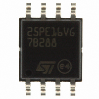
Manufacturer Part Number
M25PE16-VMW6TG
Description
IC FLASH 16MBIT 75MHZ 8SOIC
Manufacturer
NUMONYX
Series
Forté™r
Datasheet
1.M45PE16-VMP6TG.pdf
(58 pages)
Specifications of M25PE16-VMW6TG
Format - Memory
FLASH
Memory Type
FLASH
Memory Size
16M (2M x 8)
Speed
75MHz
Interface
SPI, 3-Wire Serial
Voltage - Supply
2.7 V ~ 3.6 V
Operating Temperature
-40°C ~ 85°C
Package / Case
8-SOIC (5.3mm Width), 8-SOP, 8-SOEIAJ
Package
8SOIC W
Cell Type
NOR
Density
16 Mb
Architecture
Sectored
Block Organization
Symmetrical
Typical Operating Supply Voltage
3.3 V
Sector Size
64KByte x 32
Timing Type
Synchronous
Interface Type
Serial-SPI
Lead Free Status / RoHS Status
Lead free / RoHS Compliant
Other names
M25PE16-VMW6TGTR
Available stocks
Company
Part Number
Manufacturer
Quantity
Price
Company:

Part Number:
M25PE16-VMW6TG
Manufacturer:
MAXIM
Quantity:
14 500
Company:
Part Number:
M25PE16-VMW6TG
Manufacturer:
Numonyx
Quantity:
15 000
Part Number:
M25PE16-VMW6TG
Manufacturer:
ST
Quantity:
20 000


Instructions
6
20/58
Instructions
All instructions, addresses and data are shifted in and out of the device, most significant bit
first.
Serial data input (D) is sampled on the first rising edge of Serial Clock (C) after Chip Select
(S) is driven Low. Then, the one-byte instruction code must be shifted in to the device, most
significant bit first, on serial data input (D), each bit being latched on the rising edges of
Serial Clock (C).
The instruction set is listed in
Every instruction sequence starts with a one-byte instruction code. Depending on the
instruction, this might be followed by address bytes, or by data bytes, or by both or none.
In the case of a read data bytes (READ), read data bytes at higher speed (Fast_Read), read
identification (RDID), read status register (RDSR), or read lock register (RDLR) instruction,
the shifted-in instruction sequence is followed by a data-out sequence. Chip Select (S) can
be driven High after any bit of the data-out sequence is being shifted out.
In the case of a page write (PW), page program (PP), write to lock register (WRLR), page
erase (PE), sector erase (SE), subsector erase (SSE), bulk erase (BE), write status register
(WRSR), write enable (WREN), write disable (WRDI), deep power-down (DP) or release
from deep power-down (RDP) instruction, Chip Select (S) must be driven High exactly at a
byte boundary, otherwise the instruction is rejected, and is not executed. That is, Chip
Select (S) must driven High when the number of clock pulses after Chip Select (S) being
driven Low is an exact multiple of eight.
All attempts to access the memory array during a write cycle, program cycle or erase cycle
are ignored, and the internal write cycle, program cycle or erase cycle continues unaffected.
Table
5.
M25PE16
Related parts for M25PE16-VMW6TG
Image
Part Number
Description
Manufacturer
Datasheet
Request
R

Part Number:
Description:
IC FLASH 16MBIT 75MHZ 8VFQFPN
Manufacturer:
NUMONYX
Datasheet:
Part Number:
Description:
Flash Mem Serial-SPI 3.3V 16M-Bit 2M x 8 8ns 8-Pin VFQFPN EP Tube
Manufacturer:
NUMONYX
Datasheet:
Part Number:
Description:
Flash Mem Serial-SPI 3.3V 16M-Bit 2M x 8 8ns 8-Pin SOIC W Tube
Manufacturer:
NUMONYX
Datasheet:

Part Number:
Description:
16-Mbit, page-erasable serial flash memory with byte-alterability, 75 MHz SPI bus, standard pinout
Manufacturer:
Numonyx, B.V.
Datasheet:
Part Number:
Description:
16-Mbit, page-erasable serial flash memory with byte-alterability, 75 MHz SPI bus, standard pinout
Manufacturer:
Numonyx, B.V.
Datasheet:
Part Number:
Description:
16-Mbit, page-erasable serial flash memory with byte-alterability, 75 MHz SPI bus, standard pinout
Manufacturer:
Numonyx, B.V.
Datasheet:
Part Number:
Description:
16-Mbit, page-erasable serial flash memory with byte-alterability, 75 MHz SPI bus, standard pinout
Manufacturer:
Numonyx, B.V.
Datasheet:
Part Number:
Description:
Numonyx� Embedded Flash Memory J3 V. D
Manufacturer:
Numonyx
Datasheet: