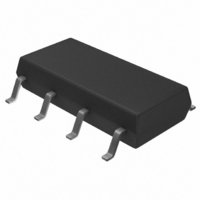
S-24CS04AFJ-TB-G Seiko Instruments, S-24CS04AFJ-TB-G Datasheet - Page 19

S-24CS04AFJ-TB-G
Manufacturer Part Number
S-24CS04AFJ-TB-G
Description
IC EEPROM 4KBIT 400KHZ 8SOP
Manufacturer
Seiko Instruments
Datasheet
1.S-24CS01AFT-TB-G.pdf
(47 pages)
Specifications of S-24CS04AFJ-TB-G
Format - Memory
EEPROMs - Serial
Memory Type
EEPROM
Memory Size
4K (512 x 8)
Speed
400kHz
Interface
I²C, 2-Wire Serial
Voltage - Supply
1.8 V ~ 5.5 V
Operating Temperature
-40°C ~ 85°C
Package / Case
8-SOP
Organization
512 x 8
Interface Type
2-Wire
Maximum Clock Frequency
0.4 MHz
Supply Voltage (max)
5.5 V
Supply Voltage (min)
1.8 V
Maximum Operating Current
4 mA
Maximum Operating Temperature
+ 85 C
Mounting Style
SMD/SMT
Minimum Operating Temperature
- 40 C
Operating Supply Voltage
5.5 V
Lead Free Status / RoHS Status
Lead free / RoHS Compliant
Available stocks
Company
Part Number
Manufacturer
Quantity
Price
Part Number:
S-24CS04AFJ-TB-G
Manufacturer:
SEK
Quantity:
20 000
Rev.4.5
8. Address Increment Timing
Write Inhibition Function at Low Power Voltage
The S-24CS01A/02A/04A/08A have a detection circuit for low power voltage. The detection circuit cancels
a write instruction when the power voltage is low or the power switch is on. The detection voltage is 1.75 V
typically and the release voltage is 2.05 V typically, the hysteresis of approximate 0.3 V thus exists. (See
Figure 21 .)
When a low power voltage is detected, a write instruction is canceled at the reception of a stop condition.
When the power voltage lowers during a data transmission or a write operation, the data at the address of
the operation is not assured.
The timing for the automatic address increment is the falling edge of the SCL clock for the 8th bit of the
read data in read operation and the falling edge of the SCL clock for the 8th bit of the received data in write
operation.
SCL
SDA
SCL
SDA
_00
Power supply voltage
R / W=1
R / W=0
8
8
Figure 19 Address Increment Timing in Reading
Figure 20 Address Increment Timing in Writing
Figure 21 Operation at low power voltage
ACK Output
ACK Output
Detection voltage (-V
9
9
1.75 V typ.
Seiko Instruments Inc.
D7 Output
D7 Input
DET
1
1
)
0.3 V approximately
Hysteresis width
Write Instruction
cancel
2-WIRE CMOS SERIAL E
Address Increment
D0 Output
Release voltage (+V
Address Increment
D0 Input
S-24CS01A/02A/04A/08A
8
8
2.05 V typ.
ACK Output
DET
)
9
9
2
PROM
19


