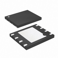
AT25DF021-MH-T Atmel, AT25DF021-MH-T Datasheet - Page 15

AT25DF021-MH-T
Manufacturer Part Number
AT25DF021-MH-T
Description
IC FLASH 2MBIT 70MHZ 8UDFN
Manufacturer
Atmel
Datasheet
1.AT25DF021-SSH-B.pdf
(41 pages)
Specifications of AT25DF021-MH-T
Format - Memory
FLASH
Memory Type
DataFLASH
Memory Size
2M (256K x 8)
Speed
70MHz
Interface
SPI, 3-Wire Serial
Voltage - Supply
2.7 V ~ 3.6 V
Operating Temperature
-40°C ~ 85°C
Package / Case
8-UDFN
Lead Free Status / RoHS Status
Lead free / RoHS Compliant
9.5
3677D–DFLASH–04/09
Global Protect/Unprotect
Registers Locked) bit of the Status Register (please refer to the Status Register description for
more details). If the Sector Protection Registers are locked, then any attempts to issue the
Unprotect Sector command will be ignored, and the device will reset the WEL bit in the Status
Register back to a logical “0” and return to the idle state once the CS pin has been deasserted.
Figure 9-4.
The Global Protect and Global Unprotect features can work in conjunction with the Protect Sec-
tor and Unprotect Sector functions. For example, a system can globally protect the entire
memory array and then use the Unprotect Sector command to individually unprotect certain sec-
tors and individually reprotect them later by using the Protect Sector command. Likewise, a
system can globally unprotect the entire memory array and then individually protect certain sec-
tors as needed.
Performing a Global Protect or Global Unprotect is accomplished by writing a certain combina-
tion of data to the Status Register using the Write Status Register Byte 1 command (see
Status Register” on page 25
mand is also used to modify the SPRL (Sector Protection Registers Locked) bit to control
hardware and software locking.
To perform a Global Protect, the appropriate WP pin and SPRL conditions must be met, and the
system must write a logical “1” to bits 5, 4, 3, and 2 of the first byte of the Status Register. Con-
versely, to perform a Global Unprotect, the same WP and SPRL conditions must be met but the
system must write a logical “0” to bits 5, 4, 3, and 2 of the first byte of the Status Register.
9-2
details the conditions necessary for a Global Protect or Global Unprotect to be performed.
SCK
SO
CS
SI
Unprotect Sector
HIGH-IMPEDANCE
MSB
0
0
0
1
1
for command execution details). The Write Status Register com-
2
OPCODE
1
3
1
4
0
5
0
6
1
7
MSB
A
8
A
9
A
10 11
A
ADDRESS BITS A23-A0
A
12
A
A
26
A
27 28
A
A
29 30
A
A
31
“Write
Table
15


