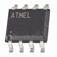
AT25DF021-SSHF-B Atmel, AT25DF021-SSHF-B Datasheet - Page 19

AT25DF021-SSHF-B
Manufacturer Part Number
AT25DF021-SSHF-B
Description
IC FLASH 2MBIT 70MHZ 8SOIC
Manufacturer
Atmel
Datasheet
1.AT25DF021-SSH-B.pdf
(41 pages)
Specifications of AT25DF021-SSHF-B
Format - Memory
FLASH
Memory Type
DataFLASH
Memory Size
2M (256K x 8)
Speed
70MHz
Interface
SPI, 3-Wire Serial
Voltage - Supply
2.3 V ~ 3.6 V
Operating Temperature
-40°C ~ 85°C
Package / Case
8-SOIC (3.9mm Width)
Memory Configuration
1024 Pages X 256 Bytes
Interface Type
Serial, SPI
Clock Frequency
66MHz
Supply Voltage Range
2.3V To 3.6V
Memory Case Style
SOIC
Rohs Compliant
Yes
Data Bus Width
8 bit
Architecture
Sectored
Timing Type
Synchronous
Access Time
6 ns
Supply Voltage (max)
3.6 V
Supply Voltage (min)
2.7 V
Maximum Operating Current
16 mA
Mounting Style
SMD/SMT
Lead Free Status / RoHS Status
Lead free / RoHS Compliant
Available stocks
Company
Part Number
Manufacturer
Quantity
Price
Part Number:
AT25DF021-SSHF-B
Manufacturer:
ATMEL/爱特梅尔
Quantity:
20 000
10. Security Commands
10.1
3677D–DFLASH–04/09
Program OTP Security Register
Table 9-5.
The device contains a specialized OTP (One-Time Programmable) Security Register that can be
used for purposes such as unique device serialization, system-level Electronic Serial Number
(ESN) storage, locked key storage, etc. The OTP Security Register is independent of the main
Flash memory array and is comprised of a total of 128 bytes of memory divided into two por-
tions. The first 64 bytes (byte locations 0 through 63) of the OTP Security Register are allocated
as a one-time user-programmable space. Once these 64 bytes have been programmed, they
cannot be erased or reprogrammed. The remaining 64 bytes of the OTP Security Register (byte
locations 64 through 127) are factory programmed by Atmel and will contain a unique value for
each device. The factory programmed data is fixed and cannot be changed.
Table 10-1.
The user-programmable portion of the OTP Security Register does not need to be erased before
it is programmed. In addition, the Program OTP Security Register command operates on the
entire 64-byte user-programmable portion of the OTP Security Register at one time. Once the
user-programmable space has been programmed with any number of bytes, the user-program-
mable space cannot be programmed again; therefore, it is not possible to only program the first
two bytes of the register and then program the remaining 62 bytes at a later time.
Before the Program OTP Security Register command can be issued, the Write Enable command
must have been previously issued to set the WEL bit in the Status Register to a logical “1”. To
program the OTP Security Register, the CS pin must first be asserted and an opcode of 9Bh
must be clocked into the device followed by the three address bytes denoting the first byte
WP
0
0
1
1
0
SPRL
One-Time User Programmable
0
1
0
1
1
Hardware and Software Locking
OTP Security Register
Hardware
Software
Locking
Locked
Locked
. . .
SPRL Change Allowed
Can be modified from 0 to 1
Locked
Can be modified from 0 to 1
Can be modified from 1 to 0
62
Security Register
Byte Number
63
64
Sector Protection Registers
Unlocked and modifiable using the
Protect and Unprotect Sector commands.
Global Protect and Unprotect can also be
performed.
Locked in current state. Protect and
Unprotect Sector commands will be
ignored. Global Protect and Unprotect
cannot be performed.
Unlocked and modifiable using the
Protect and Unprotect Sector commands.
Global Protect and Unprotect can also be
performed.
Locked in current state. Protect and
Unprotect Sector commands will be
ignored. Global Protect and Unprotect
cannot be performed.
Factory Programmed by Atmel
65
. . .
126
127
19


