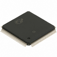
CY7C024AV-25AC Cypress Semiconductor Corp, CY7C024AV-25AC Datasheet - Page 10

CY7C024AV-25AC
Manufacturer Part Number
CY7C024AV-25AC
Description
IC SRAM 64KBIT 25NS 100LQFP
Manufacturer
Cypress Semiconductor Corp
Datasheet
1.CY7C024AV-25AC.pdf
(19 pages)
Specifications of CY7C024AV-25AC
Format - Memory
RAM
Memory Type
SRAM - Dual Port, Asynchronous
Memory Size
64K (4K x 16)
Speed
25ns
Interface
Parallel
Voltage - Supply
3 V ~ 3.6 V
Operating Temperature
0°C ~ 70°C
Package / Case
100-LQFP
Lead Free Status / RoHS Status
Contains lead / RoHS non-compliant
Other names
428-1155
Available stocks
Company
Part Number
Manufacturer
Quantity
Price
Company:
Part Number:
CY7C024AV-25AC
Manufacturer:
Cypress Semiconductor Corp
Quantity:
10 000
Part Number:
CY7C024AV-25AC
Manufacturer:
CYPRESS/赛普拉斯
Quantity:
20 000
Document #: 38-06052 Rev. *B
Switching Characteristics
Data Retention Mode
The
CY7C0241AV/0251AV/036AV are designed with battery
backup in mind. Data retention voltage and supply current are
guaranteed over temperature. The following rules ensure data
retention:
Notes:
23. For information on port-to-port delay through RAM cells from writing port to reading port, refer to Read Timing with Busy waveform.
24. Test conditions used are Load 2.
25. t
26. CE = V
t
t
t
t
t
t
t
t
t
t
t
t
t
t
t
t
t
t
t
1. Chip Enable (CE) must be held HIGH during data retention,
2. CE must be kept between V
3. The RAM can begin operation >t
HD
HZWE
LZWE
WDD
DDD
BLA
BHA
BLC
BHC
PS
WB
WH
BDD
INS
INR
SOP
SWRD
SPS
SAA
BUSY TIMING
INTERRUPT TIMING
SEMAPHORE TIMING
within V
during the power-up and power-down transitions.
minimum operating voltage (3.0V).
Parameter
[25]
BDD
[23]
[23]
[21, 22]
[21, 22]
is a calculated parameter and is the greater of t
CC
CC
, V
in
to V
= GND to V
[24]
CY7C024AV/025AV/026AV
CC
Data Hold From Write End
R/W LOW to High Z
R/W HIGH to Low Z
Write Pulse to Data Delay
Write Data Valid to Read Data Valid
BUSY LOW from Address Match
BUSY HIGH from Address Mismatch
BUSY LOW from CE LOW
BUSY HIGH from CE HIGH
Port Set-up for Priority
R/W HIGH after BUSY (Slave)
R/W HIGH after BUSY HIGH (Slave)
BUSY HIGH to Data Valid
INT Set Time
INT Reset Time
SEM Flag Update Pulse (OE or SEM)
SEM Flag Write to Read Time
SEM Flag Contention Window
SEM Address Access Time
– 0.2V.
CC
[24]
, T
A
= 25 C. This parameter is guaranteed but not tested.
CC
– 0.2V and 70% of V
Over the Operating Range
RC
after V
Description
WDD
–t
CC
PWE
reaches the
(actual) or t
CC
DDD
and
–t
SD
[18]
(actual).
(continued)
Timing
V
CE
ICC
CC
Parameter
DR1
Min.
15
10
0
3
5
0
5
5
CY7C0241AV/0251AV/036AV
CY7C0241AV/0251AV/036AV
CY7C024AV/025AV/026AV
-20
CY7C024AV/025AV/026AV
3.0V
@ VCC
Data Retention Mode
Max.
Test Conditions
20
V
12
45
30
20
20
17
20
20
20
20
CC
V
to V
CC
DR
CC
2.0V
= 2V
Min.
– 0.2V
17
12
0
0
5
0
5
5
-25
[26]
3.0V
Max.
15
50
35
20
20
20
17
25
20
20
25
Max.
Page 10 of 19
50
V
t
IH
RC
Unit
ns
ns
ns
ns
ns
ns
ns
ns
ns
ns
ns
ns
ns
ns
ns
ns
ns
ns
ns
Unit
A


