CY7C024A-25JXC Cypress Semiconductor Corp, CY7C024A-25JXC Datasheet
CY7C024A-25JXC
Specifications of CY7C024A-25JXC
Available stocks


Related parts for CY7C024A-25JXC

CY7C024A-25JXC Summary of contents
Page 1
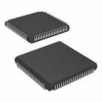
... Pin select for Master or Slave ■ Available in 84-pin (Pb-free) PLCC, 84-pin PLCC, 100-pin (Pb-free) TQFP, and 100-pin TQFP Note 1. CY7C024 and CY7C024A are functionally identical. Cypress Semiconductor Corporation Document #: 38-06035 Rev 16/18 and 8K x 16/18 Dual-Port Static RAM with SEM, INT, BUSY ...
Page 2
... BUSY is an output in master mode and an input in slave mode. 3. I/O –I/O on the CY7C0241/0251 I/O –I/O on the CY7C0241/0251 the CY7C025/0251. 12L the CY7C025/0251. 12R Document #: 38-06035 Rev. *D I/O I/O CONTROL CONTROL MEMORY ADDRESS ADDRESS ARRAY DECODER DECODER INTERRUPT CE CE SEMAPHORE L R ARBITRATION ...
Page 3
Pin Configurations (continued) 100 I/O 10L 5 I/O 6 11L I/O 12L 7 I/O 13L 8 GND 9 I/O 10 14L I/O 11 15L GND ...
Page 4
... RAM cells, I/O and address lines, and control signals (CE, OE, R/W). These control pins permit independent access for reads or writes to any location in memory. To handle simultaneous writes/reads to the same location, a BUSY pin is provided on each port. Two interrupt (INT) pins can be used for port-to-port communication ...
Page 5
... HIGH during SEM LOW). A0–2 represents the semaphore address. OE and R/W are used in the same manner as a normal memory access. When writing or reading a semaphore, the other address pins have no effect. When writing to the semaphore, only I/O written to the left port of an available semaphore, a one appears at the same semaphore address on the right port ...
Page 6
Table 3. Semaphore Operation Example I/O 0 Function No action Left port writes 0 to semaphore Right port writes 0 to semaphore Left port writes 1 to semaphore Left port writes 0 to semaphore Right port writes 1 to semaphore ...
Page 7
Maximum Ratings [10] Exceeding maximum ratings may shorten the useful life of the device. User guidelines are not tested. Storage Temperature ................................. –65°C to +150°C Ambient Temperature with Power Applied ............................................ –55°C to +125°C Supply Voltage to Ground Potential................–0.3V to ...
Page 8
Electrical Characteristics Over the Operating Range (continued) Parameter Description I Operating Current V CC Outputs Disabled I Standby Current CE SB1 (Both Ports TTL Levels Standby Current CE SB2 (One Port TTL Level ...
Page 9
Switching Characteristics Over the Operating Range Parameter Description Read Cycle t Read Cycle Time RC t Address to Data Valid AA t Output Hold From Address OHA Change [15 LOW to Data Valid ACE t OE LOW to ...
Page 10
Switching Characteristics Over the Operating Range (continued) Parameter Description [20] Busy Timing t BUSY LOW from Address BLA Match t BUSY HIGH from Address BHA Mismatch t BUSY LOW from CE LOW BLC t BUSY HIGH from CE HIGH BHC ...
Page 11
Switching Waveforms Figure 4. Read Cycle No. 1 (Either Port Address Access) ADDRESS OHA DATA OUT PREVIOUS DATA VALID Figure 5. Read Cycle No. 2 (Either Port CE/OE Access) CE and DATA OUT ...
Page 12
Switching Waveforms (continued) Figure 7. Write Cycle No. 1: R/W Controlled Timing ADDRESS OE [32,33 R/W NOTE 35 DATA OUT DATA IN Figure 8. Write Cycle No Controlled Timing ADDRESS [32,33 R/W ...
Page 13
Switching Waveforms (continued) Figure 9. Semaphore Read After Write Timing, Either Side A –A VALID ADRESS SEM I R/W OE Figure 10. Timing Diagram of Semaphore Contention A – R/W L ...
Page 14
Switching Waveforms (continued) Figure 11. Timing Diagram of Read with BUSY (M/S=HIGH) ADDRESS R R/W R DATA ADDRESS L BUSY L DATA OUTL Figure 12. Write Timing with Busy Input (M/S=LOW) R/W BUSY Note 41. CE ...
Page 15
Switching Waveforms (continued) Figure 13. Busy Timing Diagram No.1 (CE Arbitration) CE Valid First: L ADDRESS L BUSY R CE Valid First: R ADDRESS L BUSY L Figure 14. Busy Timing Diagram ...
Page 16
Switching Waveforms (continued) Left Side Sets INT : R ADDRESS WRITE FFF (1FFF CY7C025 R/W L INT R [44] t INS Right Side Clears INT : R ADDRESS R INT R ...
Page 17
... Ordering Information 4K x16 Dual-Port SRAM) ( Speed (ns) Ordering Code 15 CY7C024–15AC CY7C024-15AXC CY7C024–15JC CY7C024-15JXC 25 CY7C024–25AC CY7C024-25AXC CY7C024–25JC CY7C024A-25JXC CY7C024–25AI CY7C024-25AXI CY7C024–25JI CY7C024-25JXI 35 CY7C024–35AC CY7C024-35AXC CY7C024–35JC CY7C024-35JXC CY7C024–35AI CY7C024-35AXI CY7C024–35JI CY7C024-35JXI 55 CY7C024–55AC CY7C024-55AXC CY7C024– ...
Page 18
Ordering Information ( Dual-Port SRAM) Speed (ns) Ordering Code 25 CY7C025–25AC CY7C025-25AXC CY7C025–25JC CY7C025-25JXC CY7C025–25AI CY7C025-25AXI CY7C025–25JI CY7C025-25JXI 35 CY7C025–35AC CY7C025-35AXC CY7C025–35JC CY7C025-35JXC CY7C025–35AI CY7C025-35AXI CY7C025–35JI CY7C025-35JXI 55 CY7C025–55AC CY7C025-55AXC CY7C025–55JC CY7C025-55JXC CY7C025–55AI CY7C025-55AXI CY7C025–55JI CY7C025-55JXI Ordering Information ...
Page 19
Ordering Information ( Dual-Port SRAM) Speed (ns) Ordering Code 55 CY7C0241–55AC CY7C0241-55AXC CY7C0241–55AI CY7C0241-55AXI Dual-Port SRAM Speed (ns) Ordering Code 15 CY7C0251–15AC CY7C0251–15AXC 25 CY7C0251–25AC CY7C0251-25AXC CY7C0251–25AI CY7C0251–25AXI 35 CY7C0251–35AC CY7C0251–35AXC CY7C0251–35AI CY7C0251–35AXI 55 CY7C0251–55AC ...
Page 20
Package Diagrams Figure 16. 100-Pin Pb-Free Thin Plastic Quad Flat Pack (TQFP) A100 Figure 17. 84-Pin Pb Free Plastic Leaded Chip Carrier J83 Document #: 38-06035 Rev. *D CY7C024/024A/0241 CY7C025/0251 51-85048-*C 51-85006-*A Page [+] Feedback ...
Page 21
... Description of Change Date Change from Spec number: 38-00255 to 38-06035 12/27/02 Power up requirements added to Maximum Ratings Information Removed cross information from features section Added Lead (Pb)-Free packaging information Added CY7C024A part Updated Ordering information table PSoC Solutions General psoc.cypress.com Low Power/Low Voltage clocks.cypress.com ...