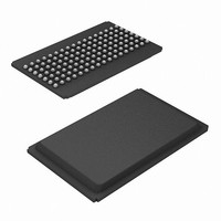
CY7C1024DV33-10BGXI Cypress Semiconductor Corp, CY7C1024DV33-10BGXI Datasheet - Page 6

CY7C1024DV33-10BGXI
Manufacturer Part Number
CY7C1024DV33-10BGXI
Description
IC SRAM 3MBIT 10NS 119BGA
Manufacturer
Cypress Semiconductor Corp
Type
Asynchronousr
Specifications of CY7C1024DV33-10BGXI
Memory Size
3M (128K x 24)
Package / Case
119-BGA
Format - Memory
RAM
Memory Type
SRAM - Asynchronous
Speed
10ns
Interface
Parallel
Voltage - Supply
3 V ~ 3.6 V
Operating Temperature
-40°C ~ 85°C
Access Time
10 ns
Maximum Clock Frequency
1 MHz
Supply Voltage (max)
3.6 V
Supply Voltage (min)
3 V
Maximum Operating Current
175 mA
Organization
128 K x 24
Maximum Operating Temperature
+ 85 C
Minimum Operating Temperature
- 40 C
Mounting Style
SMD/SMT
Number Of Ports
1
Operating Supply Voltage
3.3 V
Density
3Mb
Access Time (max)
10ns
Sync/async
Asynchronous
Architecture
Not Required
Clock Freq (max)
Not RequiredMHz
Operating Supply Voltage (typ)
3.3V
Address Bus
17b
Package Type
BGA
Operating Temp Range
-40C to 85C
Supply Current
175mA
Operating Supply Voltage (min)
3V
Operating Supply Voltage (max)
3.6V
Operating Temperature Classification
Industrial
Mounting
Surface Mount
Pin Count
119
Word Size
24b
Number Of Words
128K
Lead Free Status / RoHS Status
Lead free / RoHS Compliant
Lead Free Status / RoHS Status
Lead free / RoHS Compliant, Lead free / RoHS Compliant
Available stocks
Company
Part Number
Manufacturer
Quantity
Price
Company:
Part Number:
CY7C1024DV33-10BGXI
Manufacturer:
Cypress Semiconductor Corp
Quantity:
10 000
Company:
Part Number:
CY7C1024DV33-10BGXIT
Manufacturer:
Cypress Semiconductor Corp
Quantity:
10 000
Switching Waveforms
Notes
Document Number: 001-08353 Rev. *D
13. Device is continuously selected. OE, CE = V
14. WE is HIGH for read cycle.
15. Address valid before or similar to CE transition LOW.
16. Data I/O is high impedance if OE = V
17. If CE goes HIGH simultaneously with WE going HIGH, the output remains in a high impedance state.
DATA OUT
ADDRESS
DATA OUT
CURRENT
ADDRESS
ADDRESS
DATA I/O
SUPPLY
V
WE
CE
OE
CE
CC
PREVIOUS DATA VALID
HIGH IMPEDANCE
t
PU
Figure 3. Read Cycle No. 1 (Address Transition Controlled)
IH
t
.
LZCE
IL
Figure 4. Read Cycle No. 2 (OE Controlled)
Figure 5. Write Cycle No. 1 (CE Controlled)
t
t
.
LZOE
ACE
t
SA
t
OHA
50%
t
DOE
t
AA
t
AW
t
RC
t
WC
t
PWE
t
RC
RC
DATA VALID
t
SCE
t
t
SD
SCE
DATA VALID
[3, 14, 15]
[3, 16, 17]
t
HD
[13, 14]
DATA VALID
t
HZOE
t
HA
t
HZCE
CY7C1024DV33
t
PD
50%
IMPEDANCE
HIGH
Page 6 of 11
ICC
ISB
[+] Feedback


