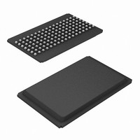
CY7C1024DV33-10BGXI Cypress Semiconductor Corp, CY7C1024DV33-10BGXI Datasheet - Page 5

CY7C1024DV33-10BGXI
Manufacturer Part Number
CY7C1024DV33-10BGXI
Description
IC SRAM 3MBIT 10NS 119BGA
Manufacturer
Cypress Semiconductor Corp
Type
Asynchronousr
Specifications of CY7C1024DV33-10BGXI
Memory Size
3M (128K x 24)
Package / Case
119-BGA
Format - Memory
RAM
Memory Type
SRAM - Asynchronous
Speed
10ns
Interface
Parallel
Voltage - Supply
3 V ~ 3.6 V
Operating Temperature
-40°C ~ 85°C
Access Time
10 ns
Maximum Clock Frequency
1 MHz
Supply Voltage (max)
3.6 V
Supply Voltage (min)
3 V
Maximum Operating Current
175 mA
Organization
128 K x 24
Maximum Operating Temperature
+ 85 C
Minimum Operating Temperature
- 40 C
Mounting Style
SMD/SMT
Number Of Ports
1
Operating Supply Voltage
3.3 V
Density
3Mb
Access Time (max)
10ns
Sync/async
Asynchronous
Architecture
Not Required
Clock Freq (max)
Not RequiredMHz
Operating Supply Voltage (typ)
3.3V
Address Bus
17b
Package Type
BGA
Operating Temp Range
-40C to 85C
Supply Current
175mA
Operating Supply Voltage (min)
3V
Operating Supply Voltage (max)
3.6V
Operating Temperature Classification
Industrial
Mounting
Surface Mount
Pin Count
119
Word Size
24b
Number Of Words
128K
Lead Free Status / RoHS Status
Lead free / RoHS Compliant
Lead Free Status / RoHS Status
Lead free / RoHS Compliant, Lead free / RoHS Compliant
Available stocks
Company
Part Number
Manufacturer
Quantity
Price
Company:
Part Number:
CY7C1024DV33-10BGXI
Manufacturer:
Cypress Semiconductor Corp
Quantity:
10 000
Company:
Part Number:
CY7C1024DV33-10BGXIT
Manufacturer:
Cypress Semiconductor Corp
Quantity:
10 000
AC Switching Characteristics
Over the Operating Range
Data Retention Characteristics
Over the Operating Range
Data Retention Waveform
Document Number: 001-08353 Rev. *D
Notes
Write Cycle
t
t
t
t
t
t
t
t
t
t
V
I
t
t
9. The internal write time of the memory is defined by the overlap of CE
10. The minimum write cycle time for Write Cycle No. 3 (WE controlled, OE LOW) is the sum of t
11. Tested initially and after any design or process changes that may affect these parameters.
12. Full device operation requires linear V
WC
SCE
AW
HA
SA
PWE
SD
HD
LZWE
HZWE
CCDR
CDR
R
Parameter
DR
[12]
Parameter
initiate a write. The transition of any of these signals terminate the write. The input data setup and hold timing is referenced to the leading edge of the signal that
terminates the write.
[11]
V
CE
CC
[9, 10]
V
Data Retention Current
Chip Deselect to Data Retention Time
Operation Recovery Time
CC
Write Cycle Time
CE active LOW to Write End
Address Setup to Write End
Address Hold from Write End
Address Setup to Write Start
WE Pulse Width
Data Setup to Write End
Data Hold from Write End
WE HIGH to Low Z
WE LOW to High Z
for Data Retention
Description
[5]
CC
ramp from V
[7]
[7]
t
CDR
3.0V
(continued)
DR
[3]
to V
Description
CC(min)
V
V
CC
IN
> V
> 50 s or stable at V
= 2V, CE > V
1
DATA RETENTION MODE
and CE
CC
– 0.2V or V
2
V
and CE
Conditions
DR
CC
>
3
2V
– 0.2V,
LOW and WE LOW. Chip enables must be active and WE must be LOW to
CC(min)
IN
HZWE
< 0.2V
> 50 s.
[3]
and t
SD
.
3.0V
Min
5.5
t
10
R
7
7
0
0
7
0
3
Min
t
RC
2
0
–10
CY7C1024DV33
Typ
Max
5
Max
25
Page 5 of 11
Unit
ns
ns
ns
ns
ns
ns
ns
ns
ns
ns
Unit
mA
ns
ns
V
[+] Feedback


