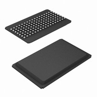
CY7C1024DV33-10BGXI Cypress Semiconductor Corp, CY7C1024DV33-10BGXI Datasheet - Page 4

CY7C1024DV33-10BGXI
Manufacturer Part Number
CY7C1024DV33-10BGXI
Description
IC SRAM 3MBIT 10NS 119BGA
Manufacturer
Cypress Semiconductor Corp
Type
Asynchronousr
Specifications of CY7C1024DV33-10BGXI
Memory Size
3M (128K x 24)
Package / Case
119-BGA
Format - Memory
RAM
Memory Type
SRAM - Asynchronous
Speed
10ns
Interface
Parallel
Voltage - Supply
3 V ~ 3.6 V
Operating Temperature
-40°C ~ 85°C
Access Time
10 ns
Maximum Clock Frequency
1 MHz
Supply Voltage (max)
3.6 V
Supply Voltage (min)
3 V
Maximum Operating Current
175 mA
Organization
128 K x 24
Maximum Operating Temperature
+ 85 C
Minimum Operating Temperature
- 40 C
Mounting Style
SMD/SMT
Number Of Ports
1
Operating Supply Voltage
3.3 V
Density
3Mb
Access Time (max)
10ns
Sync/async
Asynchronous
Architecture
Not Required
Clock Freq (max)
Not RequiredMHz
Operating Supply Voltage (typ)
3.3V
Address Bus
17b
Package Type
BGA
Operating Temp Range
-40C to 85C
Supply Current
175mA
Operating Supply Voltage (min)
3V
Operating Supply Voltage (max)
3.6V
Operating Temperature Classification
Industrial
Mounting
Surface Mount
Pin Count
119
Word Size
24b
Number Of Words
128K
Lead Free Status / RoHS Status
Lead free / RoHS Compliant
Lead Free Status / RoHS Status
Lead free / RoHS Compliant, Lead free / RoHS Compliant
Available stocks
Company
Part Number
Manufacturer
Quantity
Price
Company:
Part Number:
CY7C1024DV33-10BGXI
Manufacturer:
Cypress Semiconductor Corp
Quantity:
10 000
Company:
Part Number:
CY7C1024DV33-10BGXIT
Manufacturer:
Cypress Semiconductor Corp
Quantity:
10 000
AC Switching Characteristics
Over the Operating Range
Notes
Document Number: 001-08353 Rev. *D
Read Cycle
t
t
t
t
t
t
t
t
t
t
t
t
4. Valid SRAM operation does not occur until the power supplies have reached the minimum operating V
5. Test conditions assume signal transition time of 3 ns or less, timing reference levels of 1.5V, and input pulse levels of 0 to 3.0V. Test conditions for the read cycle use
6. t
7. t
8. These parameters are guaranteed by design and are not tested.
power
RC
AA
OHA
ACE
DOE
LZOE
HZOE
LZCE
HZCE
PU
PD
V
output loading as shown in part a) of
voltage.
*Capacitive Load consists of all
components of the test environment
Parameter
OUTPUT
POWER
HZOE
DD
[6]
, normal SRAM operation can begin including reduction in V
, t
HZCE
gives the minimum amount of time that the power supply is at typical V
, t
HZWE
V
Read Cycle Time
Address to Data Valid
Data Hold from Address Change
CE Active LOW to Data Valid
OE LOW to Data Valid
OE LOW to Low Z
OE HIGH to High Z
CE Active LOW to Low Z
CE Deselect HIGH to High Z
CE Active LOW to Power Up
CE Deselect HIGH to Power Down
, t
Z 0 = 50
CC
LZOE
(Typical) to the First Access
, t
LZCE
(a)
[5]
, and t
Rise Time > 1V/ns
Figure
LZWE
30 pF*
50
[7]
2, unless specified otherwise.
are specified with a load capacitance of 5 pF as in part (b) of
[7]
GND
3.0V
Figure 2. AC Test Loads and Waveform
[3, 7]
V
[3, 7]
TH
[3, 8]
[3]
Description
= 1.5V
DD
[3, 8]
to the data retention (V
10%
90%
All input pulses
CC
(c)
values until the first memory access is performed.
CCDR
, 2.0V) voltage.
DD
90%
(3.0V). 100 s (t
Figure
10%
[4]
Fall Time:> 1V/ns
2. Transition is measured 200 mV from steady state
OUTPUT
*
and scope
Including jig
Min
100
3.3V
10
3
1
3
0
power
) after reaching the minimum operating
–10
5 pF*
CY7C1024DV33
Max
10
10
10
R1 317
5
5
5
(b)
Page 4 of 11
351
Unit
R2
s
ns
ns
ns
ns
ns
ns
ns
ns
ns
ns
ns
[+] Feedback


