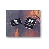
SST49LF080A-33-4C-WHE Microchip Technology, SST49LF080A-33-4C-WHE Datasheet - Page 18

SST49LF080A-33-4C-WHE
Manufacturer Part Number
SST49LF080A-33-4C-WHE
Description
IC FLASH SER LPC 8MBIT 32TSOP
Manufacturer
Microchip Technology
Datasheets
1.SST49LF080A-33-4C-NHE.pdf
(49 pages)
2.SST49LF080A-33-4C-NHE.pdf
(2 pages)
3.SST49LF080A-33-4C-NHE.pdf
(2 pages)
Specifications of SST49LF080A-33-4C-WHE
Memory Type
FLASH
Memory Size
8M (1M x 8)
Operating Temperature
0°C ~ 85°C
Package / Case
32-TSOP
Format - Memory
FLASH
Speed
33MHz
Interface
Parallel
Voltage - Supply
3 V ~ 3.6 V
Data Bus Width
8 bit
Architecture
Sectored
Interface Type
Parallel, Serial
Supply Voltage (max)
3.6 V
Supply Voltage (min)
3 V
Maximum Operating Current
12 mA
Mounting Style
SMD/SMT
Organization
4 KB x 256
Lead Free Status / RoHS Status
Lead free / RoHS Compliant
Lead Free Status / RoHS Status
Lead free / RoHS Compliant, Lead free / RoHS Compliant
Available stocks
Company
Part Number
Manufacturer
Quantity
Price
Company:
Part Number:
SST49LF080A-33-4C-WHE
Manufacturer:
SST
Quantity:
1 815
Part Number:
SST49LF080A-33-4C-WHE
Manufacturer:
SST
Quantity:
20 000
Data Sheet
Write Operation Status Detection
The SST49LF080A devices provide two software means to
detect the completion of a Write (Program or Erase) cycle,
in order to optimize the system Write cycle time. The soft-
ware detection includes two status bits: Data# Polling D[7]
and Toggle Bit D[6]. The End-of-Write detection mode is
enabled after the rising edge of WE# which initiates the
internal Program or Erase operation.
The actual completion of the nonvolatile write is asynchro-
nous with the system; therefore, either a Data# Polling or
Toggle Bit read may be simultaneous with the completion
of the Write cycle. If this occurs, the system may possibly
get an erroneous result, i.e., valid data may appear to con-
flict with either D[7] or D[6]. In order to prevent spurious
rejection, if an erroneous result occurs, the software routine
should include a loop to read the accessed location an
additional two (2) times. If both reads are valid, then the
device has completed the Write cycle, otherwise the rejec-
tion is valid.
Data# Polling (DQ
When the SST49LF080A device is in the internal Program
operation, any attempt to read DQ
plement of the true data. Once the Program operation is
completed, DQ
TABLE 10: Operation Modes Selection (PP Mode)
©2006 Silicon Storage Technology, Inc.
Mode
Read
Program
Erase
Reset
Write Inhibit
Product Identification
1. X can be V
2. Device ID = 5BH for SST49LF080A
IL
7
or V
will produce true data. Note that even
7
IH
)
, but no other value.
RST#
V
V
V
V
V
V
X
IH
IH
IH
IH
IH
IL
7
will produce the com-
OE#
V
V
V
V
V
X
X
IH
IH
IL
IL
IL
WE#
V
V
V
V
V
X
X
18
IH
IH
IH
IL
IL
though DQ
completion of an internal Write operation, the remaining
data outputs may still be invalid: valid data on the entire
data bus will appear in subsequent successive Read
cycles after an interval of 1 µs. During internal Erase opera-
tion, any attempt to read DQ
internal Erase operation is completed, DQ
‘1’. The Data# Polling is valid after the rising edge of fourth
WE# pulse for Program operation. For Sector-, Block-, or
Chip-Erase, the Data# Polling is valid after the rising edge
of sixth WE# pulse. See Figure 20 for Data# Polling timing
diagram and Figure 35 for a flowchart. Proper status will
not be given using Data# Polling if the address is in the
invalid range.
Toggle Bit (DQ
During the internal Program or Erase operation, any con-
secutive attempts to read DQ
and ‘1’s, i.e., toggling between 0 and 1. When the internal
Program or Erase operation is completed, the toggling will
stop. The device is then ready for the next operation. The
Toggle Bit is valid after the rising edge of fourth WE# pulse
for Program operation. For Sector-, Block-, or Chip-Erase,
the Toggle Bit is valid after the rising edge of sixth WE#
pulse. See Figure 21 for Toggle Bit timing diagram and Fig-
ure 35 for a flowchart.
DQ
D
D
X
High Z
High Z/D
High Z/D
Manufacturer’s ID (BFH)
Device ID
1
OUT
IN
7
may have valid data immediately following the
OUT
OUT
2
6
)
7
6
will produce a ‘0’. Once the
Address
A
A
Sector or Block address,
XXH for Chip-Erase
X
X
X
See Table 11
will produce alternating ‘0’s
8 Mbit LPC Flash
IN
IN
SST49LF080A
S71235-02-000
7
will produce a
T10.0 1235
5/06


