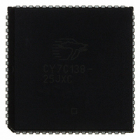
CY7C138-25JXC Cypress Semiconductor Corp, CY7C138-25JXC Datasheet - Page 6

CY7C138-25JXC
Manufacturer Part Number
CY7C138-25JXC
Description
IC SRAM 32KBIT 25NS 68PLCC
Manufacturer
Cypress Semiconductor Corp
Type
Asynchronousr
Datasheet
1.CY7C138-25JXC.pdf
(21 pages)
Specifications of CY7C138-25JXC
Memory Size
32K (4K x 8)
Package / Case
68-PLCC
Format - Memory
RAM
Memory Type
SRAM - Dual Port, Asynchronous
Speed
25ns
Interface
Parallel
Voltage - Supply
4.5 V ~ 5.5 V
Operating Temperature
0°C ~ 70°C
Access Time
25 ns
Supply Voltage (max)
5.5 V
Supply Voltage (min)
4.5 V
Maximum Operating Current
180 mA
Maximum Operating Temperature
+ 70 C
Minimum Operating Temperature
0 C
Mounting Style
SMD/SMT
Number Of Ports
2
Operating Supply Voltage
5 V
Lead Free Status / RoHS Status
Lead free / RoHS Compliant
Lead Free Status / RoHS Status
Lead free / RoHS Compliant, Lead free / RoHS Compliant
Other names
428-2148
CY7C138-25JXC
CY7C138-25JXC
Available stocks
Company
Part Number
Manufacturer
Quantity
Price
Company:
Part Number:
CY7C138-25JXC
Manufacturer:
Cypress Semiconductor Corp
Quantity:
10 000
Switching Characteristics
Document #: 38-06037 Rev. *G
t
t
t
t
t
t
t
t
t
t
t
t
t
t
t
t
t
t
t
t
t
t
t
Notes
AW
HA
SA
PWE
SD
HD
HZWE
LZWE
WDD
DDD
BLA
BHA
BLC
BHC
PS
WB
WH
BDD
INS
INR
SOP
SWRD
SPS
11. Test conditions used are Load 3.
12. This parameter is guaranteed but not tested.
13. For information on part-to-part delay through RAM cells from writing port to reading port, refer to Read Timing with Port-to-Port Delay waveform.
14. Test conditions used are Load 2.
15. t
BUSY TIMING
INTERRUPT TIMING
SEMAPHORE TIMING
BDD
[15]
[13]
[13]
[11,12]
[11,12]
Parameter
is a calculated parameter and is the greater of t
[14]
[14]
Address setup to write end
Address hold from write end
Address setup to write start
Write pulse width
Data setup to write end
Data hold from write end
R/W LOW to High Z
R/W HIGH to Low Z
Write pulse to data delay
Write data valid to read data valid
BUSY LOW from address match
BUSY HIGH from address mismatch
BUSY LOW from CE LOW
BUSY HIGH from CE HIGH
Port setup for priority
R/W LOW after BUSY LOW
R/W HIGH after BUSY HIGH
BUSY HIGH to data valid
INT set time
INT reset time
SEM flag update pulse (OE or SEM)
SEM flag write to read time
SEM flag contention window
Over the Operating Range
WDD
– t
PWE
Description
(actual) or t
DDD
[7]
– t
(continued)
SD
(actual).
Min
20
20
15
20
10
2
0
0
–
3
–
–
–
–
–
–
5
0
–
–
–
5
5
7C138-25
Note 15
Max
15
50
30
20
20
20
20
25
25
–
–
–
–
–
–
–
–
–
–
–
–
–
CY7C138
Page 6 of 21
Unit
ns
ns
ns
ns
ns
ns
ns
ns
ns
ns
ns
ns
ns
ns
ns
ns
ns
ns
ns
ns
ns
ns
ns
[+] Feedback


