CY7C138-25JXI Cypress Semiconductor Corp, CY7C138-25JXI Datasheet
CY7C138-25JXI
Specifications of CY7C138-25JXI
Available stocks


Related parts for CY7C138-25JXI


CY7C138-25JXI Summary of contents
Page 1
... Document #: 38-06037 Rev 8/9 Dual-Port Static RAM Functional Description The CY7C138 is a high speed CMOS dual-port static RAM. Various arbitration schemes are included on the CY7C138 to handle situations when multiple processors access the same piece of data. Two ports are provided permitting independent, asynchronous access for reads and writes to any location in memory ...
Page 2
... Interrupts ................................................................... 14 Busy .......................................................................... 14 Master/Slave ............................................................. 14 \ Document #: 38-06037 Rev. *G Semaphore Operation ............................................... 14 Ordering Information ...................................................... Dual-Port SRAM .............................................. 17 Ordering Code Definition ........................................... 17 Package Diagram ............................................................ 18 Acronyms ........................................................................ 19 Document Conventions ................................................. 19 Units of Measure ....................................................... 19 Document History Page ................................................. 20 Sales, Solutions, and Legal Information ...................... 21 Worldwide Sales and Design Support ....................... 21 Products .................................................................... 21 PSoC Solutions ......................................................... 21 CY7C138 Page [+] Feedback ...
Page 3
... FFE and is cleared when left L port reads location FFE. INT is set when left port writes location FFF and is cleared R when right port reads location FFF. Busy flag Master or slave select Power Ground Commercial Commercial CY7C138 ...
Page 4
... CC V > V – < 0 One port > V – 0 > V – 0 < 0.2 V, Active IN [5] Port outputs MAX CY7C138 Ambient V CC Temperature + ± 10% – + ± 10% 7C138-25 Unit Min Max 2.4 – – 0.4 2.2 – – 0.8 A – ...
Page 5
... V TH (b) Thé venin Equivalent ( Load 1) All Input Pulses 3.0 V 90% 90% 10% 10% GND < < [7] Description is less than t and t is less than t HZCE LZCE HZOE CY7C138 Max Unit 893 Output 347 (c) Three-State Delay (Load 3) 7C138-25 Unit Min Max 25 – ns – ...
Page 6
... For information on part-to-part delay through RAM cells from writing port to reading port, refer to Read Timing with Port-to-Port Delay waveform. 14. Test conditions used are Load 2. 15 calculated parameter and is the greater of t BDD Document #: 38-06037 Rev. *G [7] (continued) Description – t (actual – t (actual). WDD PWE DDD SD CY7C138 7C138-25 Unit Min Max 20 – – – – – ...
Page 7
... Figure 3. Read Cycle No. 1 (Either Port Address Access) Address t OHA Data Out Previous Data Valid Notes 16. R/W is HIGH for read cycle. 17. Device is continuously selected CE = LOW and OE = LOW. This waveform cannot be used for semaphore reads Document #: 38-06037 Rev CY7C138 [16, 17] Data Valid Page [+] Feedback ...
Page 8
... L, SEM = H when accessing RAM SEM = L when accessing semaphores. L 22. BUSY = HIGH for the writing port. 23 LOW Document #: 38-06037 Rev ACE t DOE Data Valid t WC Match t PWE t SD VALID Match t WDD CY7C138 [18, 19, 20, 21] t HZCE t HZOE t PD [22, 23 DDD Valid Page [+] Feedback ...
Page 9
... Data I/O pins enter high impedance when OE is held LOW during write. Document #: 38-06037 Rev SCE PWE t SD Data Valid High Impedance SCE PWE Data Valid t HZWE High Impedance allow the I/O drivers to turn off and data to be PWE HZWE SD CY7C138 [24, 25, 26 LZOE [24, 26, 27 LZWE Page [+] Feedback ...
Page 10
... SPS Document #: 38-06037 Rev Valid Address SCE SOP t SD Data Valid PWE t SWRD t SOP Read Cycle Match t SPS Match = CE = HIGH L CY7C138 [28] t OHA t ACE Data Valid OUT t DOE [29, 30, 31] Page [+] Feedback ...
Page 11
... Figure 10. Timing Diagram of Read with BUSY (M/S = HIGH) Address R R/W R Data Address L BUSY L Data OUTL Figure 11. Write Timing with Busy Input (M/S=LOW) R/W BUSY Note 32 LOW Document #: 38-06037 Rev Match t PWE t SD Valid Match t BLA t WDD t PWE CY7C138 [32 BHA t BDD t DDD Valid Page [+] Feedback ...
Page 12
... BUSY will be asserted. PS Document #: 38-06037 Rev. *G Address Match BLC Address Match BLC Address Mismatch t t BLA BHA Address Mismatch t t BLA BHA CY7C138 [33] t BHC t BHC [33] Page [+] Feedback ...
Page 13
... R deasserted first 35 depends on which enable pin (CE or R/W INS INR L Document #: 38-06037 Rev. *G Figure 14. Interrupt Timing Diagrams t WC Write FFF t [34 [35] INR t WC Write FFE t [34 [35] INR ) is asserted last. L CY7C138 t RC Read FFF t RC Read FFE Page [+] Feedback ...
Page 14
... Architecture The CY7C138 consists of an array of 4K words of 8 bits each of dual-port RAM cells, I/O and address lines, and control signals (CE, OE, R/W). These control pins permit independent access for reads or writes to any location in memory. To handle simultaneous writes and reads to the same location, a BUSY pin is provided on each port. Two interrupt (INT) pins can be used for port– ...
Page 15
... FFF I/O Left I/O Right 0-7 0 CY7C138 Operation Right Port INT R 0- FFE FFF Status Semaphore free Left port obtains semaphore Right side is denied access Right port is granted access to semaphore No change. Left port is denied access Left port obtains semaphore No port accessing semaphore address ...
Page 16
... Ambient Temperature (°C) Typical Access Time Change vs. Output Loading 30.0 25.0 20.0 15 ° 200 400 600 800 1000 Capacitance (pF) CY7C138 Output Source Current vs. Output Voltage 200 160 120 ° 125 0 1.0 2.0 3.0 4.0 Output Voltage (V) Output Sink Current vs ...
Page 17
... Ordering Information 4K x8 Dual-Port SRAM Speed Ordering Code (ns) 25 CY7C138-25JXC CY7C138-25JXI Ordering Code Definition CY7C XXX - Document #: 38-06037 Rev. *G Package Package Type Diagram 51-85005 68-Pin Plastic Leaded Chip Carrier (Pb-free) 51-85005 68-Pin Plastic Leaded Chip Carrier (Pb-free) Temperature Range Commercial Industrial ...
Page 18
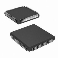
... Package Diagram Figure 16. 68-Pin Plastic Leaded Chip Carrier (51-85005) Document #: 38-06037 Rev. *G CY7C138 51-85005 *B Page [+] Feedback ...
Page 19
... TTL transistor transistor logic Document #: 38-06037 Rev. *G Document Conventions Units of Measure Symbol Unit of Measure ns nano seconds V Volts µA micro Amperes mA milli Amperes Ohms mV milli Volts MHz Mega Hertz pF pico Farad W Watts °C degree Celcius CY7C138 Page [+] Feedback ...
Page 20
... See ECN Added Pb-Free Logo Added Pb-Free parts to ordering information: CY7C138-15JXC, CY7C138-25JXC, CY7C139-25JXC 12/17/08 Added CY7C138-25JXI part Removed CY7C139 from the Ordering information table 03/12/2009 Corrected title in the Document History table 06/04/2009 Corrected defective Logic Block diagram, Pinouts and Package diagrams 03/24/10 Removed inactive parts ...
Page 21
... Cypress against all charges. Use may be limited by and subject to the applicable Cypress software license agreement. Document #: 38-06037 Rev. *G All products and company names mentioned in this document may be the trademarks of their respective holders. cypress.com/go/plc Revised December 2, 2010 CY7C138 PSoC Solutions psoc.cypress.com/solutions PSoC 1 | PSoC 3 ...