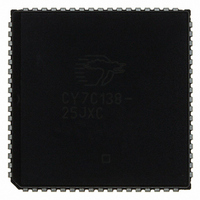
CY7C138-25JXC Cypress Semiconductor Corp, CY7C138-25JXC Datasheet - Page 10

CY7C138-25JXC
Manufacturer Part Number
CY7C138-25JXC
Description
IC SRAM 32KBIT 25NS 68PLCC
Manufacturer
Cypress Semiconductor Corp
Type
Asynchronousr
Datasheet
1.CY7C138-25JXC.pdf
(21 pages)
Specifications of CY7C138-25JXC
Memory Size
32K (4K x 8)
Package / Case
68-PLCC
Format - Memory
RAM
Memory Type
SRAM - Dual Port, Asynchronous
Speed
25ns
Interface
Parallel
Voltage - Supply
4.5 V ~ 5.5 V
Operating Temperature
0°C ~ 70°C
Access Time
25 ns
Supply Voltage (max)
5.5 V
Supply Voltage (min)
4.5 V
Maximum Operating Current
180 mA
Maximum Operating Temperature
+ 70 C
Minimum Operating Temperature
0 C
Mounting Style
SMD/SMT
Number Of Ports
2
Operating Supply Voltage
5 V
Lead Free Status / RoHS Status
Lead free / RoHS Compliant
Lead Free Status / RoHS Status
Lead free / RoHS Compliant, Lead free / RoHS Compliant
Other names
428-2148
CY7C138-25JXC
CY7C138-25JXC
Available stocks
Company
Part Number
Manufacturer
Quantity
Price
Company:
Part Number:
CY7C138-25JXC
Manufacturer:
Cypress Semiconductor Corp
Quantity:
10 000
Switching Waveforms
Notes
Document #: 38-06037 Rev. *G
28. CE = HIGH for the duration of the above timing (both write and read cycle).
29. I/O
30. Semaphores are reset (available to both ports) at cycle start.
31. If t
SPS
0R
A
0
SEM
= I/O
–A
R/W
I/O
is violated, the semaphore will definitely be obtained by one side or the other, but there is no guarantee which side will control the semaphore.
A
OE
A
0R
0L
2
0
SEM
SEM
R/W
R/W
0L
–A
–A
= LOW (request semaphore); CE
2R
2L
R
R
L
L
t
SA
(continued)
Figure 8. Semaphore Read After Write Timing, Either Side
Figure 9. Timing Diagram of Semaphore Contention
Valid Address
t
AW
Write Cycle
R
t
t
PWE
SCE
= CE
t
SD
Data
L
= HIGH
t
t
Match
SPS
Match
IN
HA
Valid
t
HD
t
SWRD
t
SOP
t
SOP
Read Cycle
t
AA
Valid Address
t
ACE
t
DOE
[29, 30, 31]
Data
[28]
OUT
Valid
t
OHA
CY7C138
Page 10 of 21
[+] Feedback


