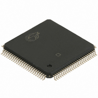
CY7C024AV-25AXC Cypress Semiconductor Corp, CY7C024AV-25AXC Datasheet - Page 7

CY7C024AV-25AXC
Manufacturer Part Number
CY7C024AV-25AXC
Description
IC SRAM 64KBIT 25NS 100LQFP
Manufacturer
Cypress Semiconductor Corp
Type
Asynchronousr
Datasheet
1.CY7C024AV-25AXC.pdf
(20 pages)
Specifications of CY7C024AV-25AXC
Memory Size
64K (4K x 16)
Package / Case
100-LQFP
Format - Memory
RAM
Memory Type
SRAM - Dual Port, Asynchronous
Speed
25ns
Interface
Parallel
Voltage - Supply
3 V ~ 3.6 V
Operating Temperature
0°C ~ 70°C
Access Time
25 ns
Supply Voltage (max)
3.6 V
Supply Voltage (min)
3 V
Maximum Operating Current
165 mA
Maximum Operating Temperature
+ 70 C
Minimum Operating Temperature
0 C
Mounting Style
SMD/SMT
Number Of Ports
2
Operating Supply Voltage
3.3 V
Memory Configuration
4K X 16
Supply Voltage Range
3V To 3.6V
Memory Case Style
TQFP
No. Of Pins
100
Operating Temperature Range
0°C To +70°C
Rohs Compliant
Yes
Lead Free Status / RoHS Status
Lead free / RoHS Compliant
Lead Free Status / RoHS Status
Lead free / RoHS Compliant, Lead free / RoHS Compliant
Other names
428-1790
CY7C024AV-25AXC
CY7C024AV-25AXC
Available stocks
Company
Part Number
Manufacturer
Quantity
Price
Company:
Part Number:
CY7C024AV-25AXC
Manufacturer:
TI
Quantity:
4 155
Company:
Part Number:
CY7C024AV-25AXC
Manufacturer:
Cypress Semiconductor Corp
Quantity:
10 000
Part Number:
CY7C024AV-25AXC
Manufacturer:
CYPRESS/赛普拉斯
Quantity:
20 000
Company:
Part Number:
CY7C024AV-25AXCT
Manufacturer:
Cypress Semiconductor Corp
Quantity:
10 000
Table 1. Non-Contending Read/Write
Table 2. Interrupt Operation Example (assumes BUSY
Table 3. Semaphore Operation Example
Document #: 38-06052 Rev. *M
Set Right INT
Reset Right INT
Set Left INT
Reset Left INT
No action
Left port writes 0 to semaphore
Right port writes 0 to semaphore
Left port writes 1 to semaphore
Left port writes 0 to semaphore
Right port writes 1 to semaphore
Left port writes 1 to semaphore
Right port writes 0 to semaphore
Right port writes 1 to semaphore
Left port writes 0 to semaphore
Left port writes 1 to semaphore
Notes
10. See
11. If BUSY
12. If BUSY
13. See
CE
H
H
H
X
X
X
X
L
L
L
L
L
L
L
L
Function
Functional Description
Functional Description
R
L
R/W
=L, then no change.
=L, then no change.
H
H
H
H
H
X
X
X
X
X
L
Function
L
L
L
Flag
R
L
Flag
R
Flag
Flag
OE
X
X
X
X
X
H
X
X
X
X
L
L
L
L
L
Inputs
on page 5 for specific highest memory locations by device.
on page 5 for specific addresses by device.
R/W
X
X
X
L
UB
X
H
H
H
X
X
H
X
H
X
L
L
L
L
L
L
CE
IO
X
X
L
L
L
LB
0
X
H
H
H
X
X
H
X
H
X
L
L
L
L
L
–IO
1
0
0
1
1
0
1
1
1
0
1
17
OE
X
X
X
L
Left
Left Port
L
SEM
H
H
H
H
H
H
H
H
X
L
L
L
L
L
L
IO
1FFE
0
High Z
High Z
Data In
High Z
Data In
Data Out
High Z
Data Out
High Z
Data Out
Data Out
Data In
Data In
A
FFF
–IO
0L–13L
L
X
X
1
1
1
0
0
1
1
0
1
1
1
17
[13]
= BUSY
IO
[13]
Right
9
–IO
17
R
Semaphore-free
No change. Right side has no write access to semaphore
Right port obtains semaphore token
No change. Left port has no write access to semaphore
Left port obtains semaphore token
Semaphore-free
Right port has semaphore token
Semaphore free
Semaphore-free
Left Port has semaphore token
Left port has semaphore token
= HIGH)
Outputs
INT
H
L
X
X
[11]
[12]
L
High Z
High Z
High Z
Data In
Data In
High Z
Data Out
Data Out
High Z
Data Out
Data Out
Data In
Data In
[10]
CY7C024AV/024BV/025AV/026AV
R/W
IO
X
X
X
L
0
R
–IO
CY7C0241AV/0251AV/036AV
8
CE
X
X
L
L
R
Deselected: Power Down
Deselected: Power Down
Write to Upper Byte Only
Write to Lower Byte Only
Write to Both Bytes
Read Upper Byte Only
Read Lower Byte Only
Read Both Bytes
Outputs Disabled
Read Data in Semaphore Flag
Read Data in Semaphore Flag
Write D
Write D
Not Allowed
Not Allowed
Status
OE
X
L
X
X
Right Port
R
IN0
IN0
1FFE (or 1/3FFE)
FFF (or 1/3FFF)
into Semaphore Flag
into Semaphore Flag
Operation
A
0R–13R
X
X
Page 7 of 20
INT
H
L
[12]
X
X
[11]
R
[+] Feedback


