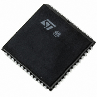
PSD834F2V-15J STMicroelectronics, PSD834F2V-15J Datasheet - Page 47

PSD834F2V-15J
Manufacturer Part Number
PSD834F2V-15J
Description
IC FLASH 2MBIT 150NS 52PLCC
Manufacturer
STMicroelectronics
Datasheet
1.PSD813F2VA-20JI.pdf
(109 pages)
Specifications of PSD834F2V-15J
Format - Memory
FLASH
Memory Type
FLASH
Memory Size
2M (256K x 8)
Speed
150ns
Interface
Parallel
Voltage - Supply
3 V ~ 3.6 V
Operating Temperature
0°C ~ 70°C
Package / Case
52-PLCC
Lead Free Status / RoHS Status
Lead free / RoHS Compliant
Other names
497-2010-5
Available stocks
Company
Part Number
Manufacturer
Quantity
Price
Company:
Part Number:
PSD834F2V-15J
Manufacturer:
STMicroelectronics
Quantity:
3
Company:
Part Number:
PSD834F2V-15J
Manufacturer:
STMicroelectronics
Quantity:
10 000
80C251
The Intel 80C251 MCU features a user-configu-
rable bus interface with four possible bus configu-
rations, as shown in
The first configuration is 80C31-compatible, and
the bus interface to the PSD is identical to that
shown in
third configurations have the same bus connection
as shown in Figure 22. There is only one Read
Strobe (PSEN) connected to CNTL1 on the PSD.
The A16 connection to PA0 allows for a larger ad-
dress input to the PSD. The fourth configuration is
shown in
connected to CNTL1 and Program Select Enable
(PSEN) is connected to CNTL2.
Figure 22. Interfacing the PSD with the 80C251, with One READ Input
Note: 1. The A16 and A17 connections are optional.
RESET
RESET
2. In non-Page-Mode, AD7-AD0 connects to ADIO7-ADIO0.
Figure 23., page
Figure 21., page
13
16
35
20
14
15
17
10
21
11
2
3
4
5
6
7
8
9
80C251SB
P3.3/INT1
P3.4/T0
RST
EA
P1.0
P1.1
P1.2
P1.3
P1.4
P1.5
P1.6
P1.7
P3.0/RXD
P3.1/TXD
P3.2/INT0
P3.5/T1
X1
X2
Table 18., page
48. Read Strobe (RD) is
RD/A16
46. The second and
PSEN
P0.0
P0.1
P0.2
P0.3
P0.4
P0.5
P0.6
P0.7
P2.0
P2.1
P2.2
P2.3
P2.4
P2.5
P2.6
P2.7
ALE
WR
43
42
41
40
39
38
37
24
25
27
33
32
18
19
36
26
28
29
30
31
RESET
48.
AD12
AD14
A0
A1
A2
A3
A4
A5
A6
A7
AD8
AD9
AD10
AD11
AD13
AD15
ALE
RD
WR
A16
Doc ID 10552 Rev 3
The 80C251 has two major operating modes:
Page mode and Non-page mode. In Non-page
mode, the data is multiplexed with the lower ad-
dress byte, and Address Strobe (ALE/AS, PD0) is
active in every bus cycle. In Page mode, data (D7-
D0) is multiplexed with address (A15-A8). In a bus
cycle where there is a Page hit, Address Strobe
(ALE/AS, PD0) is not active and only addresses
(A7-A0) are changing. The PSD supports both
modes. In Page Mode, the PSD bus timing is iden-
tical to Non-Page Mode except the address hold
time and setup time with respect to Address
Strobe (ALE/AS, PD0) is not required. The PSD
access time is measured from address (A7-A0)
valid to data in valid.
A0
A1
A2
A3
A4
A5
A6
A7
AD8
AD9
AD10
AD11
AD12
AD13
AD14
AD15
30
31
32
33
34
35
36
37
39
40
41
42
43
44
46
47
50
49
10
48
45
9
8
PSD
ADIO0
ADIO1
ADIO2
ADIO3
ADIO4
ADIO5
ADIO6
ADIO7
ADIO8
ADIO9
ADIO10
ADIO11
ADIO12
ADIO13
ADIO14
ADIO15
CNTL0 ( WR )
CNTL1 ( RD )
CNTL 2(PSEN)
PD0-ALE
PD1
PD2
RESET
PSD813F2V, PSD854F2V
PC2
PA0
PA1
PA2
PA3
PA4
PA5
PA6
PA7
PB0
PB1
PB2
PB3
PB4
PB5
PB6
PB7
PC0
PC1
PC3
PC4
PC5
PC6
PC7
29
28
27
25
24
23
22
19
18
17
14
13
12
11
21
7
6
5
4
3
2
52
51
20
A16 1
AI02881C
47/109
A17 1


