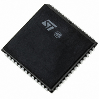
PSD834F2V-15J STMicroelectronics, PSD834F2V-15J Datasheet - Page 11

PSD834F2V-15J
Manufacturer Part Number
PSD834F2V-15J
Description
IC FLASH 2MBIT 150NS 52PLCC
Manufacturer
STMicroelectronics
Datasheet
1.PSD813F2VA-20JI.pdf
(109 pages)
Specifications of PSD834F2V-15J
Format - Memory
FLASH
Memory Type
FLASH
Memory Size
2M (256K x 8)
Speed
150ns
Interface
Parallel
Voltage - Supply
3 V ~ 3.6 V
Operating Temperature
0°C ~ 70°C
Package / Case
52-PLCC
Lead Free Status / RoHS Status
Lead free / RoHS Compliant
Other names
497-2010-5
Available stocks
Company
Part Number
Manufacturer
Quantity
Price
Company:
Part Number:
PSD834F2V-15J
Manufacturer:
STMicroelectronics
Quantity:
3
Company:
Part Number:
PSD834F2V-15J
Manufacturer:
STMicroelectronics
Quantity:
10 000
Pin Name
Reset
PC0
PC1
PB0
PB1
PB2
PB3
PB4
PB5
PB6
PB7
PA0
PA1
PA2
PA3
PA4
PA5
PA6
PA7
Pin
48
29
28
27
25
24
23
22
21
52
51
20
19
7
6
5
4
3
2
Type
I/O
I/O
I/O
I/O
I
Resets I/O Ports, PLD macrocells and some of the Configuration Registers. Must be Low
at Power-up.
These pins make up Port A. These port pins are configurable and can have the following
functions:
MCU I/O – write to or read from a standard output or input port.
CPLD macrocell (McellAB0-7) outputs.
Inputs to the PLDs.
Latched address outputs (see Table 6).
Address inputs. For example, PA0-3 could be used for A0-A3 when using an 80C51XA in
burst mode.
As the data bus inputs D0-D7 for non-multiplexed address/data bus MCUs.
D0/A16-D3/A19 in M37702M2 mode.
Peripheral I/O mode.
Note: PA0-PA3 can only output CMOS signals with an option for high slew rate. However,
PA4-PA7 can be configured as CMOS or Open Drain Outputs.
These pins make up Port B. These port pins are configurable and can have the following
functions:
MCU I/O – write to or read from a standard output or input port.
CPLD macrocell (McellAB0-7 or McellBC0-7) outputs.
Inputs to the PLDs.
Latched address outputs (see Table 6).
Note: PB0-PB3 can only output CMOS signals with an option for high slew rate. However,
PB4-PB7 can be configured as CMOS or Open Drain Outputs.
PC0 pin of Port C. This port pin can be configured to have the following functions:
MCU I/O – write to or read from a standard output or input port.
CPLD macrocell (McellBC0) output.
Input to the PLDs.
TMS Input
This pin can be configured as a CMOS or Open Drain output.
PC1 pin of Port C. This port pin can be configured to have the following functions:
MCU I/O – write to or read from a standard output or input port.
CPLD macrocell (McellBC1) output.
Input to the PLDs.
TCK Input
This pin can be configured as a CMOS or Open Drain output.
2
2
for the JTAG Serial Interface.
for the JTAG Serial Interface.
Doc ID 10552 Rev 3
Description
PSD813F2V, PSD854F2V
11/109


