CY62167EV30LL-45BVXI Cypress Semiconductor Corp, CY62167EV30LL-45BVXI Datasheet - Page 6
CY62167EV30LL-45BVXI
Manufacturer Part Number
CY62167EV30LL-45BVXI
Description
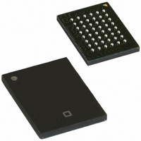
IC SRAM 16MBIT 45NS 48VFBGA
Manufacturer
Cypress Semiconductor Corp
Type
Asynchronousr
Datasheet
1.CY62167EV30LL-45BVXI.pdf
(16 pages)
Specifications of CY62167EV30LL-45BVXI
Memory Size
16M (2M x 8 or 1M x 16)
Package / Case
48-VFBGA
Format - Memory
RAM
Memory Type
SRAM
Speed
45ns
Interface
Parallel
Voltage - Supply
2.2 V ~ 3.6 V
Operating Temperature
-40°C ~ 85°C
Access Time
45 ns
Supply Voltage (max)
3.6 V
Supply Voltage (min)
2.2 V
Maximum Operating Current
30 mA
Organization
1 M x 16
Maximum Operating Temperature
+ 85 C
Minimum Operating Temperature
- 40 C
Mounting Style
SMD/SMT
Number Of Ports
1
Operating Supply Voltage
2.5 V or 3.3 V
Memory Configuration
2M X 8 / 1M X 16
Supply Voltage Range
2.2V To 3.6V
Memory Case Style
BGA
No. Of Pins
48
Rohs Compliant
Yes
Lead Free Status / RoHS Status
Lead free / RoHS Compliant
Lead Free Status / RoHS Status
Lead free / RoHS Compliant, Lead free / RoHS Compliant
Available stocks
Company
Part Number
Manufacturer
Quantity
Price
Company:

Part Number:
CY62167EV30LL-45BVXI
Manufacturer:
ON
Quantity:
6 000
Company:
Part Number:
CY62167EV30LL-45BVXI
Manufacturer:
CYPRESS
Quantity:
188
Company:
Part Number:
CY62167EV30LL-45BVXI
Manufacturer:
Cypress Semiconductor Corp
Quantity:
10 000
Part Number:
CY62167EV30LL-45BVXI
Manufacturer:
CYPRESS/赛普拉斯
Quantity:
20 000
Company:
Part Number:
CY62167EV30LL-45BVXIT
Manufacturer:
MICRON
Quantity:
1 670
Company:
Part Number:
CY62167EV30LL-45BVXIT
Manufacturer:
Cypress Semiconductor Corp
Quantity:
10 000


Data Retention Characteristics
Over the Operating Range
Document #: 38-05446 Rev. *I
Parameter
V
I
t
t
Notes
CCDR
CDR
R
13. Typical values are included for reference only and are not guaranteed or tested. Typical values are measured at V
14. Chip enables (CE
15. Tested initially and after any design or process changes that may affect these parameters.
16. Full device operation requires linear V
17. BHE.BLE is the AND of both BHE and BLE. Deselect the chip by either disabling the chip enable signals or by disabling both BHE and BLE.
DR
[16]
BHE
[15]
[14]
.
BLE
CE
V
CE
1
CC
[17]
V
Data retention current
Chip deselect to data
retention time
Operation recovery time
or
or
2
CC
for data retention
1
Description
and CE
2
), byte enables (BHE and BLE) and BYTE must be tied to CMOS levels to meet the I
CC
ramp from V
V
CE
0.2 V, V
V
0.2 V or (BHE and BLE) > V
V
CC
CC
IN
2
> V
= 1.5 V to 3.0 V, CE
= 1.5 V, CE
< 0.2 V or (BHE and BLE) > V
V
t
CC
CDR
CC
IN
DR
Figure 4. Data Retention Waveform
(min)
to V
> V
− 0.2 V or V
CC
CC
(min) > 100 μs or stable at V
1
− 0.2 V or V
> V
CC
IN
1
DATA RETENTION MODE
− 0.2 V or CE
< 0.2 V
> V
Conditions
CC
IN
CC
V
< 0.2 V
– 0.2 V,
DR
− 0.2 V or
CC
> 1.5 V
CC
2
–
(min) > 100 μs.
<
Industrial
Industrial
Auto-A All packages
SB2
CC
packages
/ I
CY62167EV30 MoBL
TSOP I
= V
48-pin
CCDR
Other
CC
V
CC
(typ), T
t
spec. Other inputs can be left floating.
R
(min)
A
Min Typ
= 25 °C.
1.5
45
–
–
–
0
–
–
–
–
–
–
[13]
Page 6 of 16
Max Unit
10
10
–
8
–
–
μA
μA
μA
ns
V
–
®
[+] Feedback
[+] Feedback
Related parts for CY62167EV30LL-45BVXI
Image
Part Number
Description
Manufacturer
Datasheet
Request
R

Part Number:
Description:
Manufacturer:
Cypress Semiconductor Corp
Datasheet:
Part Number:
Description:
Manufacturer:
Cypress Semiconductor Corp
Datasheet:
Part Number:
Description:
Manufacturer:
Cypress Semiconductor Corp
Datasheet:
Part Number:
Description:
Manufacturer:
Cypress Semiconductor Corp
Datasheet:
Part Number:
Description:
Manufacturer:
Cypress Semiconductor Corp
Datasheet: