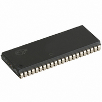
CY7C1021BN-15VXE Cypress Semiconductor Corp, CY7C1021BN-15VXE Datasheet

CY7C1021BN-15VXE
Specifications of CY7C1021BN-15VXE
Related parts for CY7C1021BN-15VXE
CY7C1021BN-15VXE Summary of contents
Page 1
... HIGH), the BHE and BLE are disabled (BHE, BLE HIGH), or during a write operation (CE LOW, WE LOW). The CY7C1021BN/CY7C10211BN is available in standard 44-pin TSOP type II and 44-pin 400-mil-wide SOJ packages. Use part number CY7C10211BN when ordering parts with and CY7C1021BN when ordering 12 ns and Data In Drivers 64K x 16 RAM Array 512 X 2048 ...
Page 2
... Selection Guide ...................................................................3 Pin Configuration ................................................................3 Pin Definitions ................................................................3 Maximum Ratings ................................................................4 Operating Range ..................................................................4 Electrical Characteristics ....................................................4 Capacitance .........................................................................5 Thermal Resistance .............................................................5 Document #: 001-06494 Rev. *C CY7C1021BN, CY7C10211BN Switching Characteristics....................................................6 Switching Waveforms .........................................................7 Truth Table ...........................................................................9 Ordering Information ...........................................................10 Ordering Code Definition ................................................10 Package Diagrams ...............................................................11 Acronyms .............................................................................12 Document History Page ......................................................13 Sales, Solutions, and Legal Information ...........................13 Worldwide Sales and Design Support ...
Page 3
... LOW, the I/O pins are allowed to behave as outputs. When deasserted HIGH, I/O pins are tristated, and act as input data pins. Ground Ground for the device. Should be connected to ground of the system. Power Supply Power supply inputs to the device. CY7C1021BN, CY7C10211BN 150 140 ...
Page 4
... Automotive-A > < Automotive-E IL MAX , Commercial/Industrial CC – 0 Commercial/Industrial (L) > V – 0 < 0 Automotive-A (L) IN Automotive-E CY7C1021BN, CY7C10211BN Ambient Temperature V [ °C to +70 ° ± 10% –40 °C to +85 °C –40 °C to +85 °C –40 °C to +125 °C -10 -12 -15 Min Max Min Max Min Max 2 ...
Page 5
... INCLUDING INCLUDING JIG AND JIG AND Rise Time: 1 V/ns Rise Time: 1 V/ns SCOPE SCOPE (b) (b) 167 Ω 167 1. CY7C1021BN, CY7C10211BN Max Unit 44-Pin SOJ 44-Pin TSOP-II °C/W 64.32 76.89 °C/W 31.03 14.28 ALL INPUT PULSES ALL INPUT PULSES ...
Page 6
... The input data setup and hold timing should be referenced to the leading edge of the signal that terminates the write. Document #: 001-06494 Rev. *C CY7C10211B-10 CY7C1021B-12 Min Max Min less than less than less than t LZCE HZOE LZOE HZBE CY7C1021BN, CY7C10211BN CY7C1021B-15 Unit Max Min Max - ...
Page 7
... Device is continuously selected. OE, CE, BHE, and BHE = V 10 HIGH for read cycle. 11. Address valid prior to or coincident with CE transition LOW. Document #: 001-06494 Rev. *C [9, 10] Figure 3. Read Cycle No OHA t RC DATA VALID 50 CY7C1021BN, CY7C10211BN DATA VALID [10, 11] t HZOE t HZCE t HZBE HIGH IMPEDANCE ICC CC 50% I ...
Page 8
... Figure 6. Write Cycle No. 2 (BLE or BHE Controlled) ADDRESS t SA BHE, BLE WE CE DATA I/O Notes 12. Data I/O is high impedance BHE and/or BLE goes HIGH simultaneously with WE going HIGH, the output remains in a high impedance state. Document #: 001-06494 Rev. *C CY7C1021BN, CY7C10211BN [12, 13 SCE PWE t BW ...
Page 9
... Read - Lower bits only Data out Read - Upper bits only Data In Write - All bits High Z Write - Lower bits only Data In Write - Upper bits only High Z Selected, outputs disabled High Z Selected, outputs disabled CY7C1021BN, CY7C10211BN LZWE Mode Power Standby (I Active (I CC Active (I ...
Page 10
... Cypress maintains a worldwide network of offices, solution centers, manufacturers’ representatives and distributors. To find the office closest to you, visit us at http://www.cypress.com/go/datasheet/offices. Speed (ns) Ordering Code 12 CY7C1021BN-12ZXC 15 CY7C1021BNL-15VXC CY7C1021BN-15ZXC CY7C1021BN-15ZXI CY7C1021BNL-15ZXI CY7C1021BNL-15ZSXA CY7C1021BN-15VXE CY7C1021BN-15ZSXE Ordering Code Definition Technology: 250 nm Speed = ns; without ns Bus Width: x16 Density: 2 Mbit ...
Page 11
... Package Diagrams Document #: 001-06494 Rev. *C CY7C1021BN, CY7C10211BN Figure 8. 44-Pin (400-Mil) Molded SOJ Figure 9. 44-Pin TSOP II 51-85082 *C 51-85087 *C Page [+] Feedback ...
Page 12
... Table 1. Acronyms Used in this Document Acronym Description BHE Byte high enable BLE Byte low enable CE Chip enable CMOS Complementary metal oxide semiconductor I/O Input/output OE Output enable SRAM Static random access memory TSOP Thin small outline package WE Write enable Document #: 001-06494 Rev. *C CY7C1021BN, CY7C10211BN Page [+] Feedback ...
Page 13
... Document History Page Document Title: CY7C1021BN, CY7C10211BN 1 Mbit (64K x 16) Static RAM Document Number: 001-06494 Submission Orig. of Rev. ECN No. Date Change ** 423877 See ECN *A 505726 See ECN *B 2897061 03/22/10 *C 2947254 06/08/10 RAME Sales, Solutions, and Legal Information Worldwide Sales and Design Support Cypress maintains a worldwide network of offices, solution centers, manufacturers’ ...


