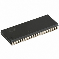
CY7C1021BN-15VXIT Cypress Semiconductor Corp, CY7C1021BN-15VXIT Datasheet

CY7C1021BN-15VXIT
Specifications of CY7C1021BN-15VXIT
Related parts for CY7C1021BN-15VXIT
CY7C1021BN-15VXIT Summary of contents
Page 1
... HIGH), the outputs are disabled (OE HIGH), the BHE and BLE are disabled (BHE, BLE HIGH), or during a write operation (CE LOW, and WE LOW). The CY7C1021BN/CY7C10211BN is available in standard 44-pin TSOP Type II and 44-pin 400-mil-wide SOJ packages. Customers should use part number CY7C10211BN when ordering parts with ...
Page 2
... When LOW, the I/O pins are allowed to behave as outputs. When deasserted HIGH, I/O pins are tri-stated, and act as input data pins. Ground Ground for the device. Should be connected to ground of the system. Power Supply Power Supply inputs to the device. CY7C1021BN CY7C10211BN 7C1021B-12 7C1021B- ...
Page 3
... Com’l / Ind’l – 0.3V, Com’l / Ind’l (L) – 0.3V, Automotive-A (L) Automotive-E Test Conditions T = 25° MHz 5.0V CC CY7C1021BN CY7C10211BN Ambient [3] Temperature ( ± 10% 0°C to +70°C –40°C to +85°C –40°C to +85°C –40°C to +125°C ...
Page 4
... Min. Max. Min less than less than t , and t HZCE LZCE HZOE LZOE CY7C1021BN CY7C10211BN 44-pin SOJ 44-pin TSOP-II Unit °C/W 64.32 76.89 °C/W 31.03 14.28 ALL INPUT PULSES ALL INPUT PULSES 90% 90% 90% 90% 10% 10% 10% 10% Fall Time: 1 V/ns 7C1021B-12 7C1021B-15 Max. ...
Page 5
... The input data set-up and hold timing should be referenced to the leading edge of the signal that terminates the write. 9. Device is continuously selected. OE, CE, BHE and/or BHE = V 10 HIGH for read cycle. Document #: 001-06494 Rev. *A 7C10211B-10 Min. Max OHA t RC DOE DATA VALID 50 CY7C1021BN CY7C10211BN 7C1021B-12 7C1021B-15 Min. Max. Min. Max. Unit DATA VALID t ...
Page 6
... DATA I/O Notes: 11. Address valid prior to or coincident with CE transition LOW. 12. Data I/O is high impedance BHE and/or BLE goes HIGH simultaneously with WE going HIGH, the output remains in a high-impedance state. Document #: 001-06494 Rev SCE PWE PWE t SCE CY7C1021BN CY7C10211BN Page [+] Feedback ...
Page 7
... Read - All bits High Z Read - Lower bits only Data Out Read - Upper bits only Data In Write - All bits High Z Write - Lower bits only Data In Write - Upper bits only High Z Selected, Outputs Disabled High Z Selected, Outputs Disabled CY7C1021BN CY7C10211BN LZWE Mode Power Standby ( Active (I ) ...
Page 8
... Ordering Code 10 CY7C10211BN-10ZXC 12 CY7C1021BN-12VC CY7C1021BN-12VXC CY7C1021BN-12ZC CY7C1021BN-12ZXC CY7C1021BN-12VI CY7C1021BN-12VXI 15 CY7C1021BN-15VC CY7C1021BN-15VXC CY7C1021BNL-15VXC CY7C1021BN-15ZC CY7C1021BN-15ZXC CY7C1021BNL-15ZC CY7C1021BNL-15ZXC CY7C1021BN-15VI CY7C1021BN-15VXI CY7C1021BN-15ZI CY7C1021BNL-15ZI CY7C1021BN-15ZXI CY7C1021BNL-15ZXI CY7C1021BNL-15ZSXA CY7C1021BN-15VXE CY7C1021BN-15ZSXE Package Diagrams 44 1 1.120 1.130 0.095 0.115 0.023 0.045 0.033 MAX. 0.013 0.023 Document #: 001-06494 Rev. *A Package ...
Page 9
... The inclusion of Cypress products in life-support systems application implies that the manufacturer assumes all risk of such use and in doing so indemnifies Cypress against all charges. 44-Pin TSOP II (51-85087) CY7C1021BN CY7C10211BN 51-85087-*A ...
Page 10
... Document History Page Document Title: CY7C1021BN/CY7C10211BN (64K x 16) Static RAM Document Number: 001-06494 Orig. of REV. ECN NO. Issue Date Change ** 423877 See ECN *A 505726 See ECN Document #: 001-06494 Rev. *A Description of Change NXR New Data Sheet NXR Removed I parameter from DC Electrical Characteristics table. ...


