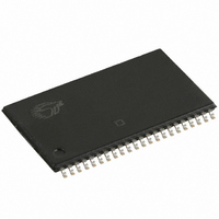
CY7C1020DV33-10ZSXI Cypress Semiconductor Corp, CY7C1020DV33-10ZSXI Datasheet - Page 3

CY7C1020DV33-10ZSXI
Manufacturer Part Number
CY7C1020DV33-10ZSXI
Description
IC SRAM 512KBIT 10NS 44TSOP
Manufacturer
Cypress Semiconductor Corp
Type
Asynchronousr
Datasheet
1.CY7C1020DV33-10ZSXI.pdf
(12 pages)
Specifications of CY7C1020DV33-10ZSXI
Memory Size
512K (32K x 16)
Package / Case
44-TSOP II
Format - Memory
RAM
Memory Type
SRAM - Asynchronous
Speed
10ns
Interface
Parallel
Voltage - Supply
3 V ~ 3.6 V
Operating Temperature
-40°C ~ 85°C
Access Time
10 ns
Supply Voltage (max)
3.6 V
Supply Voltage (min)
3 V
Maximum Operating Current
60 mA
Maximum Operating Temperature
+ 85 C
Minimum Operating Temperature
- 40 C
Mounting Style
SMD/SMT
Number Of Ports
1
Operating Supply Voltage
3.3 V
Memory Configuration
32K X 16
Supply Voltage Range
3V To 3.6V
Memory Case Style
TSOP
No. Of Pins
44
Operating Temperature Range
-40°C To +85°C
Rohs Compliant
Yes
Density
512Kb
Access Time (max)
10ns
Sync/async
Asynchronous
Architecture
Not Required
Clock Freq (max)
Not RequiredMHz
Operating Supply Voltage (typ)
3.3V
Address Bus
15b
Package Type
TSOP-II
Operating Temp Range
-40C to 85C
Supply Current
60mA
Operating Supply Voltage (min)
3V
Operating Supply Voltage (max)
3.6V
Operating Temperature Classification
Industrial
Mounting
Surface Mount
Pin Count
44
Word Size
16b
Number Of Words
32K
Lead Free Status / RoHS Status
Lead free / RoHS Compliant
Lead Free Status / RoHS Status
Lead free / RoHS Compliant, Lead free / RoHS Compliant
Other names
428-1970
CY7C1020DV33-10ZSXI
CY7C1020DV33-10ZSXI
Available stocks
Company
Part Number
Manufacturer
Quantity
Price
Part Number:
CY7C1020DV33-10ZSXI
Manufacturer:
CYPRESS/赛普拉斯
Quantity:
20 000
Document #: 38-05461 Rev. *F
AC Test Loads and Waveforms
Notes
Capacitance
Thermal Resistance
C
C
5. Tested initially and after any design or process changes that may affect these parameters.
6. AC characteristics (except High-Z) are tested using the load conditions shown in Figure (a). High-Z characteristics are tested for all speeds using the test load
Parameter
Parameter
IN
OUT
shown in Figure (c).
* CAPACITIVE LOAD CONSISTS
OF ALL COMPONENTS OF THE
TEST ENVIRONMENT
JC
JA
OUTPUT
Thermal Resistance
(Junction to Ambient)
Thermal Resistance
(Junction to Case)
Input Capacitance
Output Capacitance
[5]
Description
Description
[5]
Z = 50
(a)
1.5V
50
[6]
T
Still Air, soldered on a 3 × 4.5 inch,
four-layer printed circuit board
A
= 25C, f = 1 MHz, V
High-Z characteristics:
OUTPUT
Test Conditions
3.3V
30 pF*
Test Conditions
5 pF
CC
(c)
= 3.3V
R 317
GND
3.0V
Rise Time: 1 V/ns
351
R2
59.52
36.75
SOJ
10%
90%
ALL INPUT PULSES
(b)
Max.
TSOP II
53.91
21.24
8
8
CY7C1020DV33
Fall Time: 1 V/ns
90%
10%
Page 3 of 12
Unit
C/W
C/W
pF
pF
Unit
[+] Feedback


