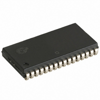
CY7C109D-10VXI Cypress Semiconductor Corp, CY7C109D-10VXI Datasheet - Page 6

CY7C109D-10VXI
Manufacturer Part Number
CY7C109D-10VXI
Description
IC SRAM 1MBIT 10NS 32SOJ
Manufacturer
Cypress Semiconductor Corp
Type
Asynchronousr
Datasheet
1.CY7C109D-10ZXI.pdf
(12 pages)
Specifications of CY7C109D-10VXI
Memory Size
1M (128K x 8)
Package / Case
32-SOJ
Format - Memory
RAM
Memory Type
SRAM - Asynchronous
Speed
10ns
Interface
Parallel
Voltage - Supply
4.5 V ~ 5.5 V
Operating Temperature
-40°C ~ 85°C
Access Time
10 ns
Supply Voltage (max)
5.5 V
Supply Voltage (min)
4.5 V
Maximum Operating Current
80 mA
Organization
128 K x 8
Maximum Operating Temperature
+ 85 C
Minimum Operating Temperature
- 40 C
Mounting Style
SMD/SMT
Number Of Ports
1
Operating Supply Voltage
5 V
Density
1Mb
Access Time (max)
10ns
Sync/async
Asynchronous
Architecture
Not Required
Clock Freq (max)
Not RequiredMHz
Operating Supply Voltage (typ)
5V
Address Bus
17b
Package Type
SOJ
Operating Temp Range
-40C to 85C
Supply Current
80mA
Operating Supply Voltage (min)
4.5V
Operating Supply Voltage (max)
5.5V
Operating Temperature Classification
Industrial
Mounting
Surface Mount
Pin Count
32
Word Size
8b
Number Of Words
128K
Lead Free Status / RoHS Status
Lead free / RoHS Compliant
Lead Free Status / RoHS Status
Lead free / RoHS Compliant, Lead free / RoHS Compliant
Other names
428-2010-5
Available stocks
Company
Part Number
Manufacturer
Quantity
Price
Data Retention Characteristics
Data Retention Waveform
Switching Waveforms
Read Cycle No. 1 (Address Transition Controlled)
Read Cycle No. 2 (OE Controlled)
Notes
Document #: 38-05468 Rev. *F
V
I
t
t
13. Full device operation requires linear V
14. Device is continuously selected. OE, CE
15. WE is HIGH for read cycle.
16. Address valid prior to or coincident with CE
CCDR
CDR
R
Parameter
DATA OUT
CURRENT
ADDRESS
DR
[13]
DATA OUT
ADDRESS
SUPPLY
[4]
V
CE
CE
OE
CC
V
CE
CC
1
2
V
Data Retention Current
Chip Deselect to Data Retention Time
Operation Recovery Time
CC
for Data Retention
PREVIOUS DATA VALID
HIGH IMPEDANCE
Description
t
PU
t
LZCE
CC
1
[15, 16]
ramp from V
= V
1
t
t
LZOE
ACE
IL
transition LOW and CE
, CE
(Over the Operating Range)
t
OHA
50%
2
t
CDR
t
= V
DOE
4.5V
DR
IH
.
to V
t
[14, 15]
CC(min)
AA
V
CE
V
CC
IN
2
1
transition HIGH.
> 50 s or stable at V
> V
t
= V
> V
RC
DATA RETENTION MODE
CC
DR
CC
– 0.3V or V
= 2.0V,
– 0.3V or CE
t
RC
V
DR
Conditions
> 2V
CC(min)
IN
DATA VALID
2
< 0.3V
> 50 s.
< 0.3V,
DATA VALID
t
HZOE
4.5V
t
R
t
HZCE
Min
t
2.0
t
PD
RC
0
CY7C1009D
50%
CY7C109D
IMPEDANCE
Max
3
Page 6 of 12
HIGH
Unit
mA
ns
ns
V
I
I
CC
SB
[+] Feedback


