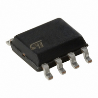
M24512-WMN6TP STMicroelectronics, M24512-WMN6TP Datasheet - Page 6

M24512-WMN6TP
Manufacturer Part Number
M24512-WMN6TP
Description
IC EEPROM 512KBIT 400KHZ 8SOIC
Manufacturer
STMicroelectronics
Specifications of M24512-WMN6TP
Format - Memory
EEPROMs - Serial
Memory Type
EEPROM
Memory Size
512K (64K x 8)
Speed
400kHz
Interface
I²C, 2-Wire Serial
Voltage - Supply
2.5 V ~ 5.5 V
Operating Temperature
-40°C ~ 85°C
Package / Case
8-SOIC (3.9mm Width)
Density
512Kb
Interface Type
Serial (I2C)
Organization
64Kx8
Access Time (max)
900ns
Frequency (max)
400KHz
Write Protection
Yes
Data Retention
40Year
Operating Supply Voltage (typ)
3.3/5V
Operating Temp Range
-40C to 85C
Supply Current
5mA
Operating Supply Voltage (min)
2.5V
Operating Supply Voltage (max)
5.5V
Operating Temperature Classification
Industrial
Mounting
Surface Mount
Pin Count
8
Lead Free Status / RoHS Status
Lead free / RoHS Compliant
Other names
497-8626-2
M24512-WMN6TP
M24512-WMN6TP
Available stocks
Company
Part Number
Manufacturer
Quantity
Price
Company:
Part Number:
M24512-WMN6TP
Manufacturer:
ELO
Quantity:
100
Company:
Part Number:
M24512-WMN6TP
Manufacturer:
STMicroelectronics
Quantity:
68 554
Part Number:
M24512-WMN6TP
Manufacturer:
ST
Quantity:
20 000
Description
1
6/39
Description
The M24512-x devices are I
(EEPROM). They are organized as 64 Kb × 8 bits.
The M24512-x can decode the type identifier code (1010) in accordance with the I
definition. The M24512-DR also decodes the type identifier code (1011) when accessing the
identification page.
The M24512-DR offers an additional Identification Page (128 bytes) which can be written
and (later) permanently locked in Read Only mode. This Identification Page can be used for
example in the assembly line, to store some application identification parameters.
The device behaves as a slave in the I
by the serial clock. Read and Write operations are initiated by a Start condition, generated
by the bus master. The Start condition is followed by a device select code and Read/Write
bit (RW) terminated by an acknowledge bit.
When writing data to the memory, the device inserts an acknowledge bit during the 9
time, following the bus master’s 8-bit transmission. When data is read by the bus master, the
bus master acknowledges the receipt of the data byte in the same way. Data transfers are
terminated by a Stop condition after an Ack for Write, and after a NoAck for Read.
Figure 1.
Table 1.
E0, E1, E2
SDA
SCL
WC
V
V
CC
SS
Signal name
Logic diagram
Signal names
2
C-compatible electrically erasable programmable memories
Doc ID 16459 Rev 19
Chip Enable
Serial Data
Serial Clock
Write Control
Supply voltage
Ground
2
C protocol, with all memory operations synchronized
Function
M24512-R, M24512-W, M24512-DR
Inputs
I/O
Input
Input
Direction
2
C bus
th
bit


