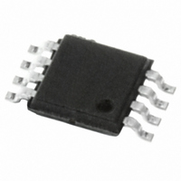
M24512-RDW6TP STMicroelectronics, M24512-RDW6TP Datasheet - Page 25

M24512-RDW6TP
Manufacturer Part Number
M24512-RDW6TP
Description
IC EEPROM 512KBIT 400KHZ 8TSSOP
Manufacturer
STMicroelectronics
Specifications of M24512-RDW6TP
Format - Memory
EEPROMs - Serial
Memory Type
EEPROM
Memory Size
512K (64K x 8)
Speed
400kHz
Interface
I²C, 2-Wire Serial
Voltage - Supply
1.8 V ~ 5.5 V
Operating Temperature
-40°C ~ 85°C
Package / Case
8-TSSOP
Organization
64 K x 8
Interface Type
I2C
Maximum Clock Frequency
0.4 MHz
Access Time
900 ns
Supply Voltage (max)
5.5 V
Supply Voltage (min)
1.8 V
Maximum Operating Current
5 mA
Maximum Operating Temperature
+ 85 C
Mounting Style
SMD/SMT
Minimum Operating Temperature
- 40 C
Operating Supply Voltage
2.5 V, 3.3 V, 5 V
Lead Free Status / RoHS Status
Lead free / RoHS Compliant
Other names
497-6349-2
Available stocks
Company
Part Number
Manufacturer
Quantity
Price
Company:
Part Number:
M24512-RDW6TP
Manufacturer:
SAMSUNG
Quantity:
10 940
Part Number:
M24512-RDW6TP
Manufacturer:
ST
Quantity:
20 000
M24256-BF, M24256-BR, M24256-BW, M24256-DR
Table 12.
1. Sampled only, not 100% tested.
2. E2,E1,E0: Input impedance when the memory is selected (after a Start condition).
Table 13.
1. Characterized value, not tested in production.
2. The device is not selected after power-up, after a Read instruction (after the Stop condition), or after the
Symbol
Symbol
I
I
V
V
Z
I
I
Z
CC0
CC1
V
completion of the internal write cycle t
I
CC
C
C
LO
OL
LI
H
L
IH
IL
IN
IN
(2)
(2)
Input leakage current
(SCL, SDA, E0, E1,
E2)
Output leakage
current
Supply current (Read)
Supply current (Write) During t
Standby supply
current
Input low voltage
(SCL, SDA, WC)
Input high voltage
(SCL, SDA)
Input high voltage
(WC, E0, E1, E2)
Output low voltage
Input capacitance (SDA)
Input capacitance (other pins)
Input impedance
(E2, E1, E0, WC)
Input impedance
(E2, E1, E0, WC)
Input parameters
DC characteristics (voltage range W)
Parameter
Parameter
(1)
Doc ID 6757 Rev 21
V
device in Standby mode
SDA in Hi-Z, external voltage applied
on SDA: V
V
(rise/fall time < 50 ns)
V
(rise/fall time < 50 ns)
Device not selected
V
= 2.5 V
V
I
OL
IN
CC
CC
IN
IN
Test conditions (see
W
= 2.1 mA, V
= V
= V
= V
= 2.5 V, f
= 5.5 V, f
(t
W
SS
SS
SS
W
is triggered by the correct decoding of a Write instruction).
, 2.5 V < V
or V
or V
or V
SS
c
c
or V
CC
CC
CC
Test condition
Table
= 400 kHz
= 400 kHz
V
V
CC
, V
, V
IN
IN
CC
= 2.5 V
(2)
CC
< 0.3V
> 0.7V
CC
CC
11)
,
= 5.5 V
< 5.5 V
Device grade 3
Device grade 6
Table 8
CC
CC
and
Min.
500
30
DC and AC parameters
0.7V
0.7V
–0.45
Min.
CC
CC
Max.
8
6
V
0.3V
CC
Max.
5
± 2
± 2
6.5
0.4
1
2
5
2
5
(1)
+0.6
CC
Unit
k
k
pF
pF
Unit
25/42
mA
mA
mA
µA
µA
µA
µA
V
V
V


