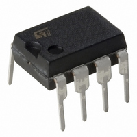
M24C02-WBN6P STMicroelectronics, M24C02-WBN6P Datasheet - Page 27

M24C02-WBN6P
Manufacturer Part Number
M24C02-WBN6P
Description
IC EEPROM 2KBIT 400KHZ 8DIP
Manufacturer
STMicroelectronics
Datasheets
1.M24C01-WMN6TP.pdf
(39 pages)
2.M24C02-WBN6P.pdf
(10 pages)
3.M24C02-WBN6P.pdf
(28 pages)
Specifications of M24C02-WBN6P
Format - Memory
EEPROMs - Serial
Memory Type
EEPROM
Memory Size
2K (256 x 8)
Speed
400kHz
Interface
I²C, 2-Wire Serial
Voltage - Supply
2.5 V ~ 5.5 V
Operating Temperature
-40°C ~ 85°C
Package / Case
8-DIP (0.300", 7.62mm)
Organization
256 K x 8
Interface Type
I2C
Maximum Clock Frequency
0.4 MHz
Access Time
900 ns
Supply Voltage (max)
5.5 V
Supply Voltage (min)
2.5 V
Maximum Operating Current
2 mA
Maximum Operating Temperature
+ 85 C
Mounting Style
Through Hole
Minimum Operating Temperature
- 40 C
Operating Supply Voltage
6.5 V
Capacitance, Input
8 pF (SDA), 6 pF (Other Pins)
Current, Input, Leakage
±2 μA
Current, Operating
2 mA
Current, Output, Leakage
±2
Data Retention
>40 yrs.
Density
2K
Package Type
PDIP8
Temperature, Operating
-40 to +85 °C
Time, Access
900 ns
Time, Fall
50 ns
Time, Rise
50 ns
Voltage, Esd
4000 V
Voltage, Input, High
3.5 to 6.5 V
Voltage, Input, Low
0.75 to 1.65 V
Voltage, Output, Low
0.4 V
Voltage, Supply
2.5 to 5.5 V
Memory Configuration
256 X 8
Clock Frequency
400kHz
Supply Voltage Range
2.5V To 5.5V
Memory Case Style
DIP
No. Of Pins
8
Rohs Compliant
Yes
Lead Free Status / RoHS Status
Lead free / RoHS Compliant
Other names
497-8584-5
M24C02-WBN6P
M24C02-WBN6P
Available stocks
Company
Part Number
Manufacturer
Quantity
Price
Part Number:
M24C02-WBN6P
Manufacturer:
ST
Quantity:
20 000
REVISION HISTORY
Table 21. Document Revision History
05-May-2000
05-May-2003
10-Dec-1999
23-Nov-2000
09-Nov-2001
17-Mar-2004
19-Feb-2001
04-Feb-2003
17-Jan-2006
18-Apr-2000
20-Apr-2001
08-Oct-2001
07-Oct-2003
30-Jul-2002
7-Oct-2005
Date
Version
2.4
2.5
2.6
3.0
3.1
3.2
3.3
3.4
3.5
3.6
3.7
4.0
5.0
6.0
7.0
TSSOP8 Turned-Die package removed (p 2 and order information)
Lead temperature added for TSSOP8 in table 2
Labelling change to Fig-2D, correction of values for ‘E’ and main caption for Tab-13
Extra labelling to Fig-2D
SBGA package information removed to an annex document
-R range changed to being the -S range, and the new -R range added
SBGA package information put back in this document
Lead Soldering Temperature in the Absolute Maximum Ratings table amended
Write Cycle Polling Flow Chart using ACK illustration updated
References to PSDIP changed to PDIP and Package Mechanical data updated
Wording brought in to line with standard glossary
Revision of DC and AC characteristics for the -S series
Ball numbers added to the SBGA connections and package mechanical illustrations
Specification of Test Condition for Leakage Currents in the DC Characteristics table
improved
Document reformatted using new template. SBGA5 package removed
TSSOP8 (3x3mm² body size) package (MSOP8) added. -L voltage range added
Document title spelt out more fully. “W”-marked devices with tw=5ms added.
-R voltage range upgraded to 400kHz working, and no longer preliminary data.
5V voltage range at temperature range 3 (-xx3) no longer preliminary data.
-S voltage range removed. -Wxx3 voltage+temp ranged added as preliminary data.
Table of contents, and Pb-free options added. Minor wording changes in Summary
Description, Power-On Reset, Memory Addressing, Read Operations. V
-0.45V. t
MLP package added. Absolute Maximum Ratings for V
Soldering temperature information clarified for RoHS compliant devices. Device grade
information clarified. Process identification letter “G” information added. 2.2-5.5V range is
removed, and 4.5-5.5V range is now Not for New Design
Product List summary table added. AEC-Q100-002 compliance. Device Grade informaton
clarified. Updated
20.
Pin numbers removed from silhouettes (see
paragraph moved to below
SIGNAL
package specifications updated (see
New definition of I
Added Ecopack® information. Updated tW=5ms for the M24Cxx-W.
W
DESCRIPTION. Test conditions for V
(max) value for -R voltage range corrected.
CC1
Device internal reset
over the whole V
Supply voltage (V
M24C16, M24C08, M24C04, M24C02, M24C01
Description of Revision
Table
CC
section,
range (see Tables 8,
16.)
Figure 1.,
CC
OL
).
Figure
updated in
Supply voltage (V
Packages).
IO
4.,
(min) and V
Figure
Table 8.
9
5.,
and 10).
Internal Device Reset
CC
Table 14.
CC
and
)
(min) changed.
added below
IL
(min) improved to
Table 9.
and
SO8N
Table
27/28


