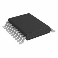
ADG3300BRUZ Analog Devices Inc, ADG3300BRUZ Datasheet - Page 7

ADG3300BRUZ
Manufacturer Part Number
ADG3300BRUZ
Description
IC XLATOR 8CH 1.2/5.5V 20TSSOP
Manufacturer
Analog Devices Inc
Datasheet
1.ADG3300BRUZ-REEL7.pdf
(20 pages)
Specifications of ADG3300BRUZ
Logic Function
Translator, Bidirectional
Number Of Bits
8
Input Type
Logic
Output Type
Logic
Data Rate
50Mbps
Number Of Channels
1
Number Of Outputs/channel
1
Differential - Input:output
No/No
Propagation Delay (max)
6ns
Voltage - Supply
1.15 V ~ 5.5 V
Operating Temperature
-40°C ~ 85°C
Package / Case
20-TSSOP
Supply Voltage
1.15 V ~ 5.5 V
No. Of Inputs
8
Propagation Delay
6ns
Logic Type
Level Translator
Supply Voltage Range
1.15V To 5.5V
Logic Case Style
TSSOP
No. Of Pins
20
Operating Temperature Range
-40°C To +85°C
High Level Output Current
-20uA
Low Level Output Current
20uA
Operating Supply Voltage (typ)
1.8/2.5/3.3/5V
Package Type
TSSOP
Operating Supply Voltage (max)
5.5V
Operating Supply Voltage (min)
1.15/1.65V
Abs. Propagation Delay Time
35ns
Mounting
Surface Mount
Pin Count
20
Operating Temperature (min)
-40C
Operating Temperature (max)
85C
Operating Temperature Classification
Industrial
Lead Free Status / RoHS Status
Lead free / RoHS Compliant
Lead Free Status / RoHS Status
Lead free / RoHS Compliant, Lead free / RoHS Compliant
Available stocks
Company
Part Number
Manufacturer
Quantity
Price
Company:
Part Number:
ADG3300BRUZ
Manufacturer:
ADI
Quantity:
1 990
Part Number:
ADG3300BRUZ
Manufacturer:
ADI/亚德诺
Quantity:
20 000
Company:
Part Number:
ADG3300BRUZ-REEL
Manufacturer:
AMS
Quantity:
3 392
PIN CONFIGURATION AND FUNCTION DESCRIPTIONS
Table 3. Pin Function Descriptions
Pin. No.
1
2
3
4
5
6
7
8
9
10
11
12
13
14
15
16
17
18
19
20
Mnemonic
A1
V
A2
A3
A4
A5
A6
A7
A8
EN
GND
Y8
Y7
Y6
Y5
Y4
Y3
Y2
V
Y1
CCA
CCY
Description
Input/Output A1. Referenced to V
Power Supply Voltage Input for the A1 to A8 I/O pins (1.15 V ≤ V
Input/Output A2. Referenced to V
Input/Output A3. Referenced to V
Input/Output A4. Referenced to V
Input/Output A5. Referenced to V
Input/Output A6. Referenced to V
Input/Output A7. Referenced to V
Input/Output A8. Referenced to V
Active High Enable Input.
Ground.
Input/Output Y8. Referenced to V
Input/Output Y7. Referenced to V
Input/Output Y6. Referenced to V
Input/Output Y5. Referenced to V
Input/Output Y4. Referenced to V
Input/Output Y3. Referenced to V
Input/Output Y2. Referenced to V
Power Supply Voltage Input for the Y1 to Y8 I/O pins (1.65 V ≤ V
Input/Output Y1. Referenced to V
V
CCA
EN
A3
A4
A1
A2
A5
A6
A7
A8
Figure 2. Pin Configuration
10
1
2
3
4
5
6
7
8
9
CCY
CCY
CCY
CCY
CCY
CCY
CCY
CCY
CCA
CCA
CCA
CCA
CCA
CCA
CCA
CCA
Rev. 0 | Page 7 of 20
(Not to Scale)
.
.
.
.
.
.
.
.
ADG3300
TOP VIEW
.
.
.
.
.
.
.
.
20
19
18
17
16
15
14
13
12
11
Y1
V
Y2
Y3
Y4
Y5
Y6
Y7
Y8
GND
CCY
CCY
CCA
≤ 5.5 V).
< V
CCY
).
ADG3300


