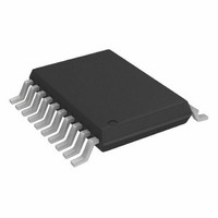
ADG3300BRUZ Analog Devices Inc, ADG3300BRUZ Datasheet

ADG3300BRUZ
Specifications of ADG3300BRUZ
Available stocks
Related parts for ADG3300BRUZ
ADG3300BRUZ Summary of contents
Page 1
FEATURES Bidirectional level translation Operates from 1. 5.5 V Low quiescent current <1 µA No direction pin APPLICATIONS Low voltage ASIC level translation Smart card readers Cell phones and cell phone cradles Portable communications devices Telecommunications equipment Network ...
Page 2
ADG3300 TABLE OF CONTENTS Specifications..................................................................................... 3 Absolute Maximum Ratings............................................................ 6 ESD Caution.................................................................................. 6 Pin Configuration and Function Descriptions............................. 7 Typical Performance Characteristics ............................................. 8 Test Circuits..................................................................................... 12 Terminology .................................................................................... 14 Theory of Operation ...................................................................... 15 Level Translator Architecture.................................................... 15 REVISION ...
Page 3
SPECIFICATIONS CCY CCA Table 1. Parameter LOGIC INPUTS/OUTPUTS A Side 3 Input High Voltage 3 Input Low Voltage Output High Voltage Output Low Voltage Three-State Pull-Down ...
Page 4
ADG3300 Parameter Y A Translation Propagation Delay Rise Time Fall Time Maximum Data Rate Channel-to-Channel Skew Part-to-Part Skew 1. 1.3 V ≤ V ≤ 3.3 V ± 0.3 V CCA CCY CCY A Y ...
Page 5
Parameter POWER REQUIREMENTS Power Supply Voltages Quiescent Power Supply Current Three-State Mode Power Supply Current 1 Temperature range is a follows: B version: −40°C to +85°C. 2 All typical values are 25°C, unless otherwise noted ...
Page 6
ADG3300 ABSOLUTE MAXIMUM RATINGS T = 25°C, unless otherwise noted. A Table 2. Parameter V to GND CCA V to GND CCY Digtal Inputs (A) Digtal Inputs ( GND Operating Temperature Range Industrial (B Version) Storage Temperature Range ...
Page 7
PIN CONFIGURATION AND FUNCTION DESCRIPTIONS Table 3. Pin Function Descriptions Pin. No. Mnemonic Description 1 A1 Input/Output A1. Referenced Power Supply Voltage Input for the I/O pins (1.15 V ≤ V CCA 3 ...
Page 8
ADG3300 TYPICAL PERFORMANCE CHARACTERISTICS 1 25° CHANNEL 0 50pF L 0 3.3V, V CCA CCY 0.7 0.6 0.5 0.4 V CCA 0.3 0.2 0 1.2V, V CCA ...
Page 9
T = 25° CHANNEL 1.8V CCA V = 3.3V CCY 7 50Mbps 6 5 30Mbps 4 3 20Mbps 2 10Mbps 1 5Mbps CAPACITIVE LOAD (pF) Figure 9. ...
Page 10
ADG3300 25° CHANNEL 9 DATA RATE = 50kbps 1.2V 1.8V CCA CCY CCA CCA ...
Page 11
T = 25°C A DATA RATE = 25Mbps 200mV/DIV Figure 21. Eye Diagram at Y Output (1 1.8 V Level Translation, 25 Mbps DATA RATE = 25Mbps CHANNEL 400mV/DIV 5ns/DIV Figure 22. Eye ...
Page 12
ADG3300 TEST CIRCUITS EN ADG3300 V CCA 0.1µ GND Figure 27 Voltages at Pin ADG3300 V CCA 0.1µ GND Figure 28 Voltages at Pin ...
Page 13
SIGNAL SOURCE R S 50Ω 90% 10% NOTES EN ADG3300 V CCA + SIGNAL 0.1µF 10µF SOURCE Z = 50Ω 50Ω T 50Ω GND V A 50% t P,A 90% ...
Page 14
ADG3300 TERMINOLOGY Table 4. Symbol Description V Logic input high voltage at Pins A1 to A8. IHA V Logic input low voltage at Pins A1 to A8. ILA V Logic output high voltage at Pins A1 to A8. OHA V ...
Page 15
THEORY OF OPERATION The ADG3300 level translator allows the level shifting necessary for data transfer in a system where multiple supply voltages are used. The device requires two supplies These supplies set the logic levels on each ...
Page 16
ADG3300 DATA RATE The maximum data rate at which the device is guaranteed to operate is a function of the V and V CCA combination and the load capacitance given by the maximum frequency of a square wave ...
Page 17
APPLICATIONS The ADG3300 is designed for digital circuits that operate at different supply voltages; therefore, logic level translation is required. The lower voltage logic signals are connected to the A pins, and the higher voltage logic signals are connected to ...
Page 18
... ADG3300 OUTLINE DIMENSIONS COPLANARITY ORDERING GUIDE Model Temperature Range 1 ADG3300BRUZ −40°C to +85°C 1 ADG3300BRUZ-REEL −40°C to +85°C 1 ADG3300BRUZ-REEL7 −40°C to +85° Pb-free part. 6.60 6.50 6. 4.50 4.40 4.30 6.40 BSC 1 10 PIN 1 0.65 BSC 1.20 MAX 0.15 0.20 ...
Page 19
NOTES Rev Page ADG3300 ...
Page 20
ADG3300 NOTES © 2005 Analog Devices, Inc. All rights reserved. Trademarks and registered trademarks are the property of their respective owners. D05061–0–4/05(0) Rev Page ...


