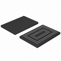
SSTUM32865ET/S,518 NXP Semiconductors, SSTUM32865ET/S,518 Datasheet - Page 8

SSTUM32865ET/S,518
Manufacturer Part Number
SSTUM32865ET/S,518
Description
IC BUFFER 1.8V 28BIT 160-TFBGA
Manufacturer
NXP Semiconductors
Specifications of SSTUM32865ET/S,518
Logic Type
1:2 Registered Buffer with Parity
Supply Voltage
1.7 V ~ 2 V
Number Of Bits
28
Operating Temperature
0°C ~ 85°C
Mounting Type
Surface Mount
Package / Case
160-TFBGA
Lead Free Status / RoHS Status
Lead free / RoHS Compliant
Other names
935284905518
SSTUM32865ET/S-T
SSTUM32865ET/S-T
SSTUM32865ET/S-T
SSTUM32865ET/S-T
Available stocks
Company
Part Number
Manufacturer
Quantity
Price
Company:
Part Number:
SSTUM32865ET/S,518
Manufacturer:
NXP Semiconductors
Quantity:
10 000
NXP memory-interface solutions
NXP DDR2 PLL and register solution
Memory interfaces
DDR2 Registered DIMM
Reset
V REF
DCKE
DODT
feedback in
DCS
CSR
Differential
Differential
CK
CK
D1
clock in
Control
DRAM
DDR2
DRAM
DDR2
DRAM
DDR2
DDR register
DDR2 PLL
DRAM
DDR2
DRAM
DDR2
Powerdown
PLL
control
SSTU32864/866*
SSTU32865**
PLL clock buffer
DDR2 registers
PCKU877
0
1
command
Address/
SPD
1D
C1
1D
C1
1D
C1
1D
C1
R
R
R
R
N+1
N
1
DRAM
DDR2
DRAM
DDR2
DRAM
DDR2
Differential
clock out 1
Differential
clock out N
Differential
feedback out
DRAM
DDR2
QCSB
QCKEA
QCKEB
QODTA
QODTB
QCSA
Q1A
Q1B
(1)
(1)
(1)
(1)
DDR2 400 – 533
Delivering steady advances in memory density and offering
speeds from 400 MT/s to 800 MT/s, DDR2 is the prevailing
standard for new memory subsystems. DDR2 registers and
PLLs use pseudo-differential SSTL_18 signaling for the address
bus (series stub terminated logic, 1.8 V), and differential
signaling for the clock, to minimize level-induced skew and
jitter. To take advantage of higher DRAM densities while
maintaining good signal integrity under heavier loading,
NXP offers a normal drive output (SSTU) and a high-drive
output (SSTUH) for each register configuration. Graphics
workstations and other systems that power-down the memory
subsystem benefit from PLLs with faster lock times, which allow
for faster sleep recovery.
}
}
}
}
}
}
}
}
SSTU32864
SSTU32865
SSTU32866
SSTUH32864
SSTUH32865
SSTUH32866
PCKU877
PCKU878
1.8-V typical supply voltage
SSTL_18 signaling
Double Data Rate (DDR)
400- to 533-MT/s data rates
200- to 267-MHz clock rates
SSTU registers with normal output drive for most common
RDIMM applications
SSTUH registers with high output drive for densely
populated or s tacked RDIMM applications
Output drivers designed for high speed, low overshoot and
undershoot, high signal integrity
1.8-V 25-bit 1:1 or 14-bit 1:2 configurable registered
buffer for DDR2 RDIMM applications
1.8-V 28-bit 1:2 registered buffer with parity for DDR2
RDIMM applications
1.8-V 25-bit 1:1 or 14-bit 1:2 configurable registered
buffer with parity for DDR2 RDIMM applications
1.8-V 25-bit 1:1 or 14-bit 1:2 configurable registered
buffer with high output drive for DDR2 RDIMM
applications
1.8-V 28-bit 1:2 registered buffer with parity and high
output drive for DDR2 RDIMM applications
1.8-V 25-bit 1:1 or 14-bit 1:2 configurable registered
buffer with parity and high output drive for DDR2
RDIMM applications
1.8-V 1:10 differential zero-delay PLL clock buffer for
DDR2 400-533 RDIMM applications
1.8-V 1:10 differential zero-delay PLL clock buffer with
fast lock time for DDR2 400-533 RDIMM applications


