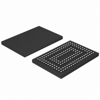
SSTUM32865ET/S,518 NXP Semiconductors, SSTUM32865ET/S,518 Datasheet - Page 7

SSTUM32865ET/S,518
Manufacturer Part Number
SSTUM32865ET/S,518
Description
IC BUFFER 1.8V 28BIT 160-TFBGA
Manufacturer
NXP Semiconductors
Specifications of SSTUM32865ET/S,518
Logic Type
1:2 Registered Buffer with Parity
Supply Voltage
1.7 V ~ 2 V
Number Of Bits
28
Operating Temperature
0°C ~ 85°C
Mounting Type
Surface Mount
Package / Case
160-TFBGA
Lead Free Status / RoHS Status
Lead free / RoHS Compliant
Other names
935284905518
SSTUM32865ET/S-T
SSTUM32865ET/S-T
SSTUM32865ET/S-T
SSTUM32865ET/S-T
Available stocks
Company
Part Number
Manufacturer
Quantity
Price
Company:
Part Number:
SSTUM32865ET/S,518
Manufacturer:
NXP Semiconductors
Quantity:
10 000
DDR 333 – 400
The higher speed grades of DDR 333-400 (333 and 400
MT/s, using 167 and 200 MHz clock rates) mean tighter timing
specifications – especially register propagation delay, PLL jitter,
and skew – to support the shorter system clock cycle. In the
case of DDR400, the supply voltage to the memory module,
and hence to the PLL and register, is increased from the typical
2.5 V ±200 mV to 2.6 V ±100 mV for higher performance.
As with all DDR speed grades, registers are available in a 1:1
configuration for the most common planar DIMM technologies
and, for stacked DRAM applications, which have a higher load
on the address bus, in 1:2 configurations.
}
}
}
}
}
PCKVF857
SSTVF16857
SSTVF16859
SSTVN16859
2.5-V typical supply voltage (2.6-V supply voltage for
DDR-400)
SSTL_2 signaling
Double Data Rate (DDR)
333- to 400-MT/s data rates
167- to 200-MHz clock rates
60- to 225-MHz differential 1:10 PLL clock driver for
DDR200 – DDR400 RDIMMs
14-bit 1:1 SSTL_2 registered driver with differential
clock inputs for DDR200 – DDR400 RDIMMs
13-bit 1:2 SSTL_2 registered driver with differential
clock inputs for stacked DDR200 – DDR400 DIMMs
13-bit 1:2 SSTL_2 registered driver with differential
clock inputs for stacked DDR200 – DDR400 DIMMs
Memory interfaces


