MC100EP57DTG ON Semiconductor, MC100EP57DTG Datasheet - Page 3
MC100EP57DTG
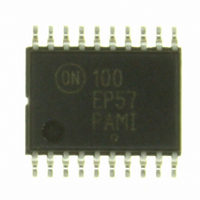
Manufacturer Part Number
MC100EP57DTG
Description
IC MUX 4:1 DIFF ECL 5V 20TSSOP
Manufacturer
ON Semiconductor
Series
100EPr
Type
Differential Digital Multiplexerr
Datasheet
1.MC10EP57DTG.pdf
(11 pages)
Specifications of MC100EP57DTG
Circuit
4 x 2:1
Independent Circuits
1
Voltage Supply Source
Dual Supply
Voltage - Supply
3 V ~ 5.5 V
Operating Temperature
-40°C ~ 85°C
Mounting Type
Surface Mount
Package / Case
20-TSSOP
Product
Decoders, Encoders, Multiplexers & Demultiplexers
Logic Family
MC100E
Number Of Lines (input / Output)
4.0 / 1.0
Propagation Delay Time
0.475 ns at 3 V to 5.5 V
Supply Voltage (max)
- 5.5 V, + 5.5 V
Supply Voltage (min)
- 3 V, + 3 V
Maximum Operating Temperature
+ 85 C
Minimum Operating Temperature
- 40 C
Mounting Style
SMD/SMT
Number Of Input Lines
4.0
Number Of Output Lines
1.0
Logical Function
Mux
Configuration
1 x 4:1
Number Of Inputs
4
Number Of Outputs
1
Operating Supply Voltage (typ)
-3.3/-5/3.3/5V
Operating Supply Voltage (min)
-3/3V
Operating Supply Voltage (max)
-5.5/5.5V
Operating Temp Range
-40C to 85C
Operating Temperature Classification
Industrial
Mounting
Surface Mount
Pin Count
20
Package Type
TSSOP
Logic Type
Multiplexer
No. Of Channels
1
Ratio
4
Supply Voltage Range
3V To 5.5V
Logic Case Style
TSSOP
No. Of Pins
20
Operating Temperature Range
-40°C To +85°C
Filter Terminals
SMD
Rohs Compliant
Yes
Lead Free Status / RoHS Status
Lead free / RoHS Compliant
Current - Output High, Low
-
Lead Free Status / Rohs Status
Lead free / RoHS Compliant
Other names
MC100EP57DTGOS
Available stocks
Company
Part Number
Manufacturer
Quantity
Price

Part Number:
MC100EP57DTG
Manufacturer:
ON/安森美
Quantity:
20 000


Stresses exceeding Maximum Ratings may damage the device. Maximum Ratings are stress ratings only. Functional operation above the
Recommended Operating Conditions is not implied. Extended exposure to stresses above the Recommended Operating Conditions may affect
device reliability.
Table 4. MAXIMUM RATINGS
Symbol
V
V
V
I
I
T
T
q
q
q
q
T
out
BB
A
stg
JA
JC
JA
JC
sol
CC
EE
I
PECL Mode Power Supply
NECL Mode Power Supply
PECL Mode Input Voltage
NECL Mode Input Voltage
Output Current
V
Operating Temperature Range
Storage Temperature Range
Thermal Resistance (Junction−to−Ambient)
Thermal Resistance (Junction−to−Case)
Thermal Resistance (Junction−to−Ambient)
Thermal Resistance (Junction−to−Case)
Wave Solder
BB
Sink/Source
Table 3. ATTRIBUTES
1. For additional information, see Application Note AND8003/D.
Internal Input Pulldown Resistor
Internal Input Pullup Resistor
ESD Protection
Moisture Sensitivity, Indefinite Time Out of Drypack (Note 1)
Flammability Rating
Transistor Count
Meets or exceeds JEDEC Spec EIA/JESD78 IC Latchup Test
Parameter
Characteristics
Pb−Free
Pb
http://onsemi.com
Oxygen Index: 28 to 34
Charged Device Model
V
V
V
V
Continuous
Surge
0 lfpm
500 lfpm
Standard Board
0 lfpm
500 lfpm
Standard Board
EE
CC
EE
CC
Human Body Model
Condition 1
= 0 V
= 0 V
= 0 V
= 0 V
Machine Model
3
TSSOP−20
QFN−20
V
V
TSSOP−20
TSSOP−20
TSSOP−20
QFN−20
QFN−20
QFN−20
I
I
v V
w V
Condition 2
Pb Pkg
Level 1
UL 94 V−0 @ 0.125 in
N/A
CC
EE
584 Devices
> 100 V
> 4 kV
> 2 kV
Value
75 kW
N/A
Pb−Free Pkg
Level 3
Level 1
−65 to +150
−40 to +85
23 to 41
Rating
± 0.5
100
140
100
265
265
−6
−6
50
47
33
18
6
6
°C/W
°C/W
°C/W
°C/W
°C/W
°C/W
Unit
mA
mA
mA
°C
°C
°C
V
V
V
V
Related parts for MC100EP57DTG
Image
Part Number
Description
Manufacturer
Datasheet
Request
R

Part Number:
Description:
MICROCOUPLER, SMALL TRANSISTOR OUTPUT
Manufacturer:
Micropac Industries, Inc.
Part Number:
Description:
Steckbare Anschlussklemmen, Raster 5,08 mm
Manufacturer:
LUMBERG [Lumberg]
Datasheet:

Part Number:
Description:
MC100-50805K
Manufacturer:
Cooper/Bussmann
Datasheet:

Part Number:
Description:
ON Semiconductor [VOLTAGE REGULATOR]
Manufacturer:
ON Semiconductor
Datasheet:
Part Number:
Description:
357-036-542-201 CARDEDGE 36POS DL .156 BLK LOPRO
Manufacturer:
ON Semiconductor
Datasheet:
Part Number:
Description:
357-036-542-201 CARDEDGE 36POS DL .156 BLK LOPRO
Manufacturer:
ON Semiconductor
Datasheet:
Part Number:
Description:
357-036-542-201 CARDEDGE 36POS DL .156 BLK LOPRO
Manufacturer:
ON Semiconductor
Datasheet:
Part Number:
Description:
357-036-542-201 CARDEDGE 36POS DL .156 BLK LOPRO
Manufacturer:
ON Semiconductor
Datasheet:
Part Number:
Description:
357-036-542-201 CARDEDGE 36POS DL .156 BLK LOPRO
Manufacturer:
ON Semiconductor
Datasheet:
Part Number:
Description:
357-036-542-201 CARDEDGE 36POS DL .156 BLK LOPRO
Manufacturer:
ON Semiconductor
Datasheet: