MC100EP57DTG ON Semiconductor, MC100EP57DTG Datasheet - Page 2
MC100EP57DTG
Manufacturer Part Number
MC100EP57DTG
Description
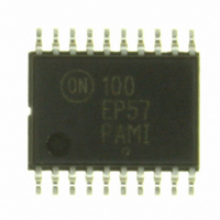
IC MUX 4:1 DIFF ECL 5V 20TSSOP
Manufacturer
ON Semiconductor
Series
100EPr
Type
Differential Digital Multiplexerr
Datasheet
1.MC10EP57DTG.pdf
(11 pages)
Specifications of MC100EP57DTG
Circuit
4 x 2:1
Independent Circuits
1
Voltage Supply Source
Dual Supply
Voltage - Supply
3 V ~ 5.5 V
Operating Temperature
-40°C ~ 85°C
Mounting Type
Surface Mount
Package / Case
20-TSSOP
Product
Decoders, Encoders, Multiplexers & Demultiplexers
Logic Family
MC100E
Number Of Lines (input / Output)
4.0 / 1.0
Propagation Delay Time
0.475 ns at 3 V to 5.5 V
Supply Voltage (max)
- 5.5 V, + 5.5 V
Supply Voltage (min)
- 3 V, + 3 V
Maximum Operating Temperature
+ 85 C
Minimum Operating Temperature
- 40 C
Mounting Style
SMD/SMT
Number Of Input Lines
4.0
Number Of Output Lines
1.0
Logical Function
Mux
Configuration
1 x 4:1
Number Of Inputs
4
Number Of Outputs
1
Operating Supply Voltage (typ)
-3.3/-5/3.3/5V
Operating Supply Voltage (min)
-3/3V
Operating Supply Voltage (max)
-5.5/5.5V
Operating Temp Range
-40C to 85C
Operating Temperature Classification
Industrial
Mounting
Surface Mount
Pin Count
20
Package Type
TSSOP
Logic Type
Multiplexer
No. Of Channels
1
Ratio
4
Supply Voltage Range
3V To 5.5V
Logic Case Style
TSSOP
No. Of Pins
20
Operating Temperature Range
-40°C To +85°C
Filter Terminals
SMD
Rohs Compliant
Yes
Lead Free Status / RoHS Status
Lead free / RoHS Compliant
Current - Output High, Low
-
Lead Free Status / Rohs Status
Lead free / RoHS Compliant
Other names
MC100EP57DTGOS
Available stocks
Company
Part Number
Manufacturer
Quantity
Price

Part Number:
MC100EP57DTG
Manufacturer:
ON/安森美
Quantity:
20 000


Table 1. PIN DESCRIPTION
*Pins will default LOW when left open.
D0 − 3*, D0 − 3*
SEL0*, SEL1*
V
Q, Q
V
V
EP
BB1
CC
EE
, V
BB2
PIN
NOTE:
ECL Differential Data Inputs
ECL MUX Select Inputs
ECL Reference Output Voltage
ECL Data Outputs
Positive Supply
Negative Supply
Exposed Pad
V
V
The Exposed Pad (EP) on package bottom must be attached to a heat−sinking conduit.
The Exposed Pad may only be electrically connected to V
20
CC
CC
1
Figure 1. 20−Lead Package (Top View) and Logic Diagram
SEL1
D0
19
Warning: All V
to Power Supply to guarantee proper operation.
D0
D1
D1
D2
D2
2
FUNCTION
SEL0
1
2
3
4
5
D0
18
3
Figure 1. QFN−20 Pinout
CC
V
D1
17
D0
20
D3
6
4
and V
CC
http://onsemi.com
V
MC10/100EP57
D3
EE
CC
19
7
D1
16
Q
5
pins must be externally connected
4:1
V
V
18
CC
2
EE
8
D2
Q
15
6
SEL1
V
Table 2. TRUTH TABLE
17
EE
9
SEL1
H
H
L
L
(Top View)
V
SEL0
V
D2
14
16
10
CC
7
BB2
EE
V
D3
13
.
8
BB1
SEL0
15
14
13
12
11
H
H
L
L
Q
Exposed Pad
V
Q
V
V
V
D3
12
9
CC
CC
BB1
BB2
V
V
10
11
EE
DATA OUT
EE
D0, D0
D1, D1
D2, D2
D3, D3
Related parts for MC100EP57DTG
Image
Part Number
Description
Manufacturer
Datasheet
Request
R

Part Number:
Description:
MICROCOUPLER, SMALL TRANSISTOR OUTPUT
Manufacturer:
Micropac Industries, Inc.
Part Number:
Description:
Steckbare Anschlussklemmen, Raster 5,08 mm
Manufacturer:
LUMBERG [Lumberg]
Datasheet:

Part Number:
Description:
MC100-50805K
Manufacturer:
Cooper/Bussmann
Datasheet:

Part Number:
Description:
ON Semiconductor [VOLTAGE REGULATOR]
Manufacturer:
ON Semiconductor
Datasheet:
Part Number:
Description:
357-036-542-201 CARDEDGE 36POS DL .156 BLK LOPRO
Manufacturer:
ON Semiconductor
Datasheet:
Part Number:
Description:
357-036-542-201 CARDEDGE 36POS DL .156 BLK LOPRO
Manufacturer:
ON Semiconductor
Datasheet:
Part Number:
Description:
357-036-542-201 CARDEDGE 36POS DL .156 BLK LOPRO
Manufacturer:
ON Semiconductor
Datasheet:
Part Number:
Description:
357-036-542-201 CARDEDGE 36POS DL .156 BLK LOPRO
Manufacturer:
ON Semiconductor
Datasheet:
Part Number:
Description:
357-036-542-201 CARDEDGE 36POS DL .156 BLK LOPRO
Manufacturer:
ON Semiconductor
Datasheet:
Part Number:
Description:
357-036-542-201 CARDEDGE 36POS DL .156 BLK LOPRO
Manufacturer:
ON Semiconductor
Datasheet: