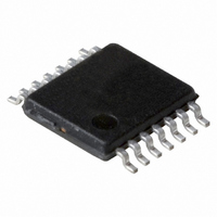
CBT3125PW,112 NXP Semiconductors, CBT3125PW,112 Datasheet - Page 4

CBT3125PW,112
Manufacturer Part Number
CBT3125PW,112
Description
IC FET BUS SWITCH QUAD 14TSSOP
Manufacturer
NXP Semiconductors
Series
74CBTr
Type
FET Bus Switchr
Datasheet
1.CBT3125DB118.pdf
(10 pages)
Specifications of CBT3125PW,112
Circuit
1 x 1:1
Independent Circuits
4
Current - Output High, Low
15mA, 64mA
Voltage Supply Source
Single Supply
Voltage - Supply
4.5 V ~ 5.5 V
Operating Temperature
-40°C ~ 85°C
Mounting Type
Surface Mount
Package / Case
14-TSSOP
Logic Family
CBT
Number Of Bits
4
Number Of Elements
4
Technology
CMOS
High Level Output Current
-128mA
Low Level Output Current
128mA
On Resistance
10Ohm
Propagation Delay Time
5.4ns
Package Type
TSSOP
Operating Temp Range
-40C to 85C
Operating Temperature Classification
Industrial
Operating Supply Voltage (min)
4.5V
Operating Supply Voltage (typ)
5V
Operating Supply Voltage (max)
5.5V
Quiescent Current
3uA
Pin Count
14
Mounting
Surface Mount
Lead Free Status / RoHS Status
Lead free / RoHS Compliant
Other names
935270670112
CBT3125PWDH
CBT3125PWDH
CBT3125PWDH
CBT3125PWDH
1. All typical values are at V
2. This is the increase in supply current for each input that is at the specified TTL voltage level rather than V
3. Measured by the voltage drop between the A and the B terminals at the indicated current through the switch. On-state resistance is
1. This parameter is warranted but not production tested. The propagation delay is based on the RC time constant of the typical on-state
Philips Semiconductors
DC ELECTRICAL CHARACTERISTICS
Over recommended operating free-air temperature range, unless otherwise noted.
NOTES:
AC CHARACTERISTICS
T
NOTE:
2001 Dec 12
amb
SYMBOL
C
Quadruple FET bus switch
SYMBOL
SYMBOL
determined by the lower of the voltages of the two (A or B) terminals.
resistance of the switch and a load capacitance of 50 pF, when driven by an ideal voltage source (zero output impedance).
IO(OFF)
V
I
V
r
= –40 to +85 C; C
C
CC
I
I
on
CC
IK
t
t
t
I
P
I
dis
pd
en
Input clamp voltage
Input leakage current
Quiescent supply current
Additional supply current per
input pin (Note 2)
Input capacitance
Power-off leakage current
Pass gate voltage
On-resistance (Note 3)
Propagation delay
Output enable time
to High and Low level
Output disable time
from High and Low level
L
= 50 pF, unless otherwise noted.
CC
PARAMETER
PARAMETER
PARAMETER
= 5 V, unless otherwise noted. T
1
control inputs
control inputs
V
I
V
V
V
V
V
one input at 3.4 V,
other inputs at V
V
V
V
V
I
V
I
V
I
amb
I
I
I
I
CC
CC
I
CC
I
CC
I
O
CC
CC
CC
CC
(INPUT)
= –18 mA
= 64 mA
= 30 mA
= –15 mA
FROM
= 5.5 V or GND
= V
= 3 V or 0
A or B
= 3 V or 0; OE = V
OE
OE
= 25 C.
= 4.5 V;
= 5.5 V;
= 5.5 V; I
= 5.5 V;
= 5.0 V; V
= 4.5 V; V
= 4.5 V; V
= 4.5 V; V
CC
CONDITIONS
4
or GND
O
I
I
I
I
= 0;
= 5.0 V
= 0 V;
= 0 V;
= 2.4 V;
CC
or GND
(OUTPUT)
CC
B or A
A or B
A or B
TO
MIN.
—
—
—
—
—
—
—
—
—
—
Min
1.0
—
V
1
CC
CC
TYP.
= 5 V
or GND.
1.7
3.4
3.8
—
—
—
—
10
5
5
1
0.5 V
Max
0.25
5.4
4.7
MAX.
CBT3125
–1.2
2.5
15
—
—
—
3
7
7
1
Product data
UNIT
UNIT
ns
ns
ns
UNIT
mA
pF
pF
V
V
A
A


