CBT3125PW,112 NXP Semiconductors, CBT3125PW,112 Datasheet - Page 3
CBT3125PW,112
Manufacturer Part Number
CBT3125PW,112
Description
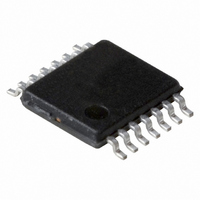
IC FET BUS SWITCH QUAD 14TSSOP
Manufacturer
NXP Semiconductors
Series
74CBTr
Type
FET Bus Switchr
Datasheet
1.CBT3125DB118.pdf
(10 pages)
Specifications of CBT3125PW,112
Circuit
1 x 1:1
Independent Circuits
4
Current - Output High, Low
15mA, 64mA
Voltage Supply Source
Single Supply
Voltage - Supply
4.5 V ~ 5.5 V
Operating Temperature
-40°C ~ 85°C
Mounting Type
Surface Mount
Package / Case
14-TSSOP
Logic Family
CBT
Number Of Bits
4
Number Of Elements
4
Technology
CMOS
High Level Output Current
-128mA
Low Level Output Current
128mA
On Resistance
10Ohm
Propagation Delay Time
5.4ns
Package Type
TSSOP
Operating Temp Range
-40C to 85C
Operating Temperature Classification
Industrial
Operating Supply Voltage (min)
4.5V
Operating Supply Voltage (typ)
5V
Operating Supply Voltage (max)
5.5V
Quiescent Current
3uA
Pin Count
14
Mounting
Surface Mount
Lead Free Status / RoHS Status
Lead free / RoHS Compliant
Other names
935270670112
CBT3125PWDH
CBT3125PWDH
CBT3125PWDH
CBT3125PWDH


Pin numbers shown are for 14-pin package-types.
1. Stresses beyond those listed under “absolute maximum ratings” may cause permanent damage to the device. These are stress ratings only,
2. The input and output negative-voltage ratings may be exceeded if the input and output clamp-current ratings are observed.
3. The package thermal impedance is calculated in accordance with JESD 51-7.
1. All unused control inputs of the device must be held at V
Philips Semiconductors
LOGIC DIAGRAM
ABSOLUTE MAXIMUM RATINGS
Over operating free-air temperature range, unless otherwise noted.
NOTES:
RECOMMENDED OPERATING CONDITIONS
NOTE:
2001 Dec 12
SYMBOL
SYMBOL
Quadruple FET bus switch
and functional operation of the device at these or any other conditions beyond those indicated under “recommended operating conditions”
is not implied. Exposure to absolute-maximum-rated conditions for extended periods may affect device reliability.
T
V
V
T
V
V
amb
V
I
CC
stg
CC
K
IH
IL
I
Figure 3. CBT3125 logic diagram (positive logic)
1OE
2OE
3OE
4OE
1A
2A
3A
4A
supply voltage range
input voltage range
continuous channel current
input clamp current
storage temperature range
supply voltage
high-level control input voltage
low-level control input voltage
operating ambient temperature in free-air
2
1
5
4
9
10
12
13
PARAMETER
PARAMETER
1
SA00564
11
3
6
8
1B
2B
3B
4B
1
CC
or GND to ensure proper device operation.
3
FUNCTION TABLE (each bus switch)
see Note 2
V
I/O
< 0
CONDITIONS
CONDITIONS
INPUT
OE
H
L
MIN.
MIN.
–0.5
–0.5
–65
–40
4.5
—
—
—
2
FUNCTION
disconnect
A = B
MAX.
MAX.
CBT3125
+150
128
–50
+85
5.5
0.8
—
7
7
Product data
UNIT
UNIT
mA
mA
V
V
V
V
V
C
C
Related parts for CBT3125PW,112
Image
Part Number
Description
Manufacturer
Datasheet
Request
R

Part Number:
Description:
Manufacturer:
NXP Semiconductors
Datasheet:
Part Number:
Description:
Cbt3125 Quadruple Fet Bus Switch
Manufacturer:
NXP Semiconductors
Datasheet:
Part Number:
Description:
NXP Semiconductors designed the LPC2420/2460 microcontroller around a 16-bit/32-bitARM7TDMI-S CPU core with real-time debug interfaces that include both JTAG andembedded trace
Manufacturer:
NXP Semiconductors
Datasheet:

Part Number:
Description:
NXP Semiconductors designed the LPC2458 microcontroller around a 16-bit/32-bitARM7TDMI-S CPU core with real-time debug interfaces that include both JTAG andembedded trace
Manufacturer:
NXP Semiconductors
Datasheet:
Part Number:
Description:
NXP Semiconductors designed the LPC2468 microcontroller around a 16-bit/32-bitARM7TDMI-S CPU core with real-time debug interfaces that include both JTAG andembedded trace
Manufacturer:
NXP Semiconductors
Datasheet:
Part Number:
Description:
NXP Semiconductors designed the LPC2470 microcontroller, powered by theARM7TDMI-S core, to be a highly integrated microcontroller for a wide range ofapplications that require advanced communications and high quality graphic displays
Manufacturer:
NXP Semiconductors
Datasheet:
Part Number:
Description:
NXP Semiconductors designed the LPC2478 microcontroller, powered by theARM7TDMI-S core, to be a highly integrated microcontroller for a wide range ofapplications that require advanced communications and high quality graphic displays
Manufacturer:
NXP Semiconductors
Datasheet:
Part Number:
Description:
The Philips Semiconductors XA (eXtended Architecture) family of 16-bit single-chip microcontrollers is powerful enough to easily handle the requirements of high performance embedded applications, yet inexpensive enough to compete in the market for hi
Manufacturer:
NXP Semiconductors
Datasheet:
Part Number:
Description:
The XA-S3 device is a member of Philips Semiconductors? XA(eXtended Architecture) family of high performance 16-bitsingle-chip microcontrollers
Manufacturer:
NXP Semiconductors
Datasheet:

Part Number:
Description:
The NXP BlueStreak LH75401/LH75411 family consists of two low-cost 16/32-bit System-on-Chip (SoC) devices
Manufacturer:
NXP Semiconductors
Datasheet:
Part Number:
Description:
The NXP LPC3130/3131 combine an 180 MHz ARM926EJ-S CPU core, high-speed USB2
Manufacturer:
NXP Semiconductors
Datasheet:
Part Number:
Description:
The NXP LPC3141 combine a 270 MHz ARM926EJ-S CPU core, High-speed USB 2
Manufacturer:
NXP Semiconductors
Part Number:
Description:
The NXP LPC3143 combine a 270 MHz ARM926EJ-S CPU core, High-speed USB 2
Manufacturer:
NXP Semiconductors

Part Number:
Description:
The NXP LPC3152 combines an 180 MHz ARM926EJ-S CPU core, High-speed USB 2
Manufacturer:
NXP Semiconductors