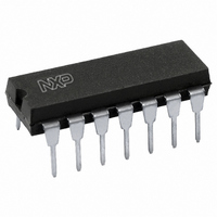
N74F164N,602 NXP Semiconductors, N74F164N,602 Datasheet - Page 4

N74F164N,602
Manufacturer Part Number
N74F164N,602
Description
IC SHIFT REGISTER 8BIT 14DIP
Manufacturer
NXP Semiconductors
Series
74Fr
Datasheet
1.N74F164D623.pdf
(10 pages)
Specifications of N74F164N,602
Package / Case
14-DIP (0.300", 7.62mm)
Logic Type
Shift Register
Function
Serial to Parallel
Output Type
Standard
Number Of Elements
1
Number Of Bits Per Element
8
Voltage - Supply
4.5 V ~ 5.5 V
Operating Temperature
-40°C ~ 85°C
Mounting Type
Through Hole
Counting Sequence
Serial to Parallel
Number Of Circuits
1
Logic Family
F
Propagation Delay Time
7 ns
Supply Voltage (max)
5.5 V
Maximum Operating Temperature
+ 70 C
Minimum Operating Temperature
0 C
Mounting Style
Through Hole
Supply Voltage (min)
4.5 V
Lead Free Status / RoHS Status
Lead free / RoHS Compliant
Lead Free Status / RoHS Status
Lead free / RoHS Compliant, Lead free / RoHS Compliant
Other names
933794740602
N74F164N
N74F164N
N74F164N
N74F164N
4. Measure I
1. For conditions shown as MIN or MAX, use the appropriate value specified under recommended operating conditions for the applicable type.
2. All typical values are at V
3. Not more than one output should be shorted at a time. For testing I
Philips Semiconductors
DC ELECTRICAL CHARACTERISTICS
(Over recommended operating free-air temperature range unless otherwise noted.)
Notes to DC electrical characteristics
APPLICATION
2000 Dec 18
techniques are preferable in order to minimize internal heating and more accurately reflect operational values. Otherwise, prolonged shorting
8-bit serial-in parallel-out shift register
SYMBOL
SYMBOL
The 74F164 can be cascaded to form synchronous shift registers of longer length.
Here, two devices are combined to form a 16-bit shift register.
of a High output may raise the chip temperature well above normal and thereby cause invalid readings in other parameter tests. In any
sequence of parameter test, I
open.
V
V
V
V
I
I
I
I
ILL
OS
CC
OH
OH
IH
OL
I
IK
I
CC
High-level output voltage
High-level out ut voltage
Low-level output voltage
Input clamp voltage
Input current at maximum input voltage
High-level input current
Low-level input current
Short-circuit output current
Supply current (total)
with the serial inputs grounded, the clock input at 2.4 V, and a momentary ground, then applied to Master Reset, and all outputs
ENABLE
CLOCK
RESET
DATA
CC
PARAMETER
PARAMETER
= 5 V, T
OS
tests should be performed last.
4
amb
Dsa
Dsb
Q0
D0
3
= 25 C.
Q1
D1
CP
Q2
D2
Q3
D3
74F164
Q4
D4
V
V
V
V
V
V
V
V
V
V
CC
CC
IH
CC
CC
IH
CC
CC
CC
CC
CC
CC
MR
Q5
D5
= MIN, I
= MIN, I
= MIN, V
= MIN, V
= MIN, I
= MAX, V
= MAX, V
= MAX, V
= MAX
= MAX
Q6
D6
OS
Q7
D7
4
OH
OL
, the use of high-speed test apparatus and/or sample-and-hold
I
IL
IL
IL
IL
= I
= MAX
I
I
I
CONDITIONS
= MAX
= 7.0 V
= 2.7 V
= 0.5 V
= MAX,
= MAX,
IK
TEST
H
Dsa
Dsb
Q0
D8
1
Q1
D9 D10 D11 D12 D13 D14 D15
10%V
10%V
5%V
5%V
Q2
CP
CC
CC
CC
CC
Q3
74F164
Q4
Q5
MR
MIN
–60
2.5
2.7
Q6
SF00716
LIMITS
Q7
–0.73
TYP
0.30
0.30
3.4
33
Product specification
2
74F164
MAX
–150
0.50
0.50
–1.2
–0.6
100
20
55
UNIT
mA
mA
mA
V
V
V
V
V
A
A


