N74F164N,602 NXP Semiconductors, N74F164N,602 Datasheet - Page 2
N74F164N,602
Manufacturer Part Number
N74F164N,602
Description
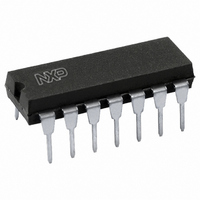
IC SHIFT REGISTER 8BIT 14DIP
Manufacturer
NXP Semiconductors
Series
74Fr
Datasheet
1.N74F164D623.pdf
(10 pages)
Specifications of N74F164N,602
Package / Case
14-DIP (0.300", 7.62mm)
Logic Type
Shift Register
Function
Serial to Parallel
Output Type
Standard
Number Of Elements
1
Number Of Bits Per Element
8
Voltage - Supply
4.5 V ~ 5.5 V
Operating Temperature
-40°C ~ 85°C
Mounting Type
Through Hole
Counting Sequence
Serial to Parallel
Number Of Circuits
1
Logic Family
F
Propagation Delay Time
7 ns
Supply Voltage (max)
5.5 V
Maximum Operating Temperature
+ 70 C
Minimum Operating Temperature
0 C
Mounting Style
Through Hole
Supply Voltage (min)
4.5 V
Lead Free Status / RoHS Status
Lead free / RoHS Compliant
Lead Free Status / RoHS Status
Lead free / RoHS Compliant, Lead free / RoHS Compliant
Other names
933794740602
N74F164N
N74F164N
N74F164N
N74F164N


through one of two inputs (Dsa, Dsb); either input can be used as an
active High enable for data entry through the other input. Both inputs
Philips Semiconductors
FEATURES
DESCRIPTION
The 74F164 is an 8-bit edge-triggered shift register with serial data
entry and an output from each of the eight stages. Data is entered
must be connected together or an unused input must be tied High.
Data shifts one place to the right on each Low-to-High transition of
the clock (CP) input, and enters into Q0 the logical AND of the two
data inputs (Dsa, Dsb) that existed one setup time before the rising
edge. A Low level on the Master Reset (MR) input overrides all
other inputs and clears the register asynchronously, forcing all
outputs Low.
ORDERING INFORMATION
INPUT AND OUTPUT LOADING AND FAN OUT TABLE
One (1.0) FAST unit load is defined as: 20 A in the High state and 0.6 mA in the Low state.
LOGIC SYMBOL
14-pin plastic DIP
2000 Dec 18
14-pin plastic SO
V
GND = Pin 7
Gated serial data inputs
Typical shift frequency of 100MHz
Asynchronous Master Reset
Buffered clock and data inputs
Fully synchronous data transfer
Industrial temperature range available (–40 to +85 C)
DESCRIPTION
CC
8-bit serial-in parallel-out shift register
= Pin 14
Dsa, Dsb
Q0 – Q7
PINS
MR
CP
8
9
CP
MR
Q0
3
Q1 Q2 Q3 Q4 Q5 Q6 Q7
4
V
5
Data inputs
Clock pulse input (active rising edge)
Master reset input (active-Low)
Data outputs
CC
Dsa
1
6 10 11 12 13
= 5 V 10%, T
COMMERCIAL RANGE
Dsb
2
SF00713
74F164N
74F164D
DESCRIPTION
amb
= 0 to +70 C
ORDER CODE
2
PIN CONFIGURATION
IEC/IEEE SYMBOL
V
CC
TYPE
74F164
= 5 V 10%, T
HIGH / LOW
74F (U.L.)
INDUSTRIAL RANGE
1.0 / 1.0
1.0 / 1.0
1.0 / 1.0
50 / 33
I74F164N
I74F164D
GND
8
9
1
2
TYPICAL f
Dsa
Dsb
Q0
Q1
Q2
Q3
amb
100MHz
1
2
3
4
5
6
7
= –40 to +85 C
R
C1/
&
max
SRG8
1D
SF00717
SF00714
14
13
12
10
11
9
8
1.0 mA / 20 mA
20 A / 0.6 mA
20 A / 0.6 mA
20 A / 0.6 mA
LOAD VALUE
CURRENT (TOTAL)
TYPICAL SUPPLY
HIGH / LOW
V
Q7
Q6
Q5
Q4
MR
CP
Product specification
10
12
13
CC
11
3
4
5
6
853-0348 25264
33 mA
74F164
DRAWING
DRAWING
SOT108-1
NUMBER
SOT27-1
Related parts for N74F164N,602
Image
Part Number
Description
Manufacturer
Datasheet
Request
R

Part Number:
Description:
Counter Shift Registers 8-BIT SIPO SHIFT REG
Manufacturer:
NXP Semiconductors
Part Number:
Description:
NXP Semiconductors designed the LPC2420/2460 microcontroller around a 16-bit/32-bitARM7TDMI-S CPU core with real-time debug interfaces that include both JTAG andembedded trace
Manufacturer:
NXP Semiconductors
Datasheet:

Part Number:
Description:
NXP Semiconductors designed the LPC2458 microcontroller around a 16-bit/32-bitARM7TDMI-S CPU core with real-time debug interfaces that include both JTAG andembedded trace
Manufacturer:
NXP Semiconductors
Datasheet:
Part Number:
Description:
NXP Semiconductors designed the LPC2468 microcontroller around a 16-bit/32-bitARM7TDMI-S CPU core with real-time debug interfaces that include both JTAG andembedded trace
Manufacturer:
NXP Semiconductors
Datasheet:
Part Number:
Description:
NXP Semiconductors designed the LPC2470 microcontroller, powered by theARM7TDMI-S core, to be a highly integrated microcontroller for a wide range ofapplications that require advanced communications and high quality graphic displays
Manufacturer:
NXP Semiconductors
Datasheet:
Part Number:
Description:
NXP Semiconductors designed the LPC2478 microcontroller, powered by theARM7TDMI-S core, to be a highly integrated microcontroller for a wide range ofapplications that require advanced communications and high quality graphic displays
Manufacturer:
NXP Semiconductors
Datasheet:
Part Number:
Description:
The Philips Semiconductors XA (eXtended Architecture) family of 16-bit single-chip microcontrollers is powerful enough to easily handle the requirements of high performance embedded applications, yet inexpensive enough to compete in the market for hi
Manufacturer:
NXP Semiconductors
Datasheet:
Part Number:
Description:
The XA-S3 device is a member of Philips Semiconductors? XA(eXtended Architecture) family of high performance 16-bitsingle-chip microcontrollers
Manufacturer:
NXP Semiconductors
Datasheet:

Part Number:
Description:
The NXP BlueStreak LH75401/LH75411 family consists of two low-cost 16/32-bit System-on-Chip (SoC) devices
Manufacturer:
NXP Semiconductors
Datasheet:
Part Number:
Description:
The NXP LPC3130/3131 combine an 180 MHz ARM926EJ-S CPU core, high-speed USB2
Manufacturer:
NXP Semiconductors
Datasheet:
Part Number:
Description:
The NXP LPC3141 combine a 270 MHz ARM926EJ-S CPU core, High-speed USB 2
Manufacturer:
NXP Semiconductors
Part Number:
Description:
The NXP LPC3143 combine a 270 MHz ARM926EJ-S CPU core, High-speed USB 2
Manufacturer:
NXP Semiconductors

Part Number:
Description:
The NXP LPC3152 combines an 180 MHz ARM926EJ-S CPU core, High-speed USB 2
Manufacturer:
NXP Semiconductors
Part Number:
Description:
The NXP LPC3154 combines an 180 MHz ARM926EJ-S CPU core, High-speed USB 2
Manufacturer:
NXP Semiconductors