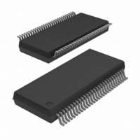
74ABT16841ADL,518 NXP Semiconductors, 74ABT16841ADL,518 Datasheet - Page 5

74ABT16841ADL,518
Manufacturer Part Number
74ABT16841ADL,518
Description
IC 20BIT BUS INTFC LATCH 56SSOP
Manufacturer
NXP Semiconductors
Series
74ABTr
Datasheet
1.74ABT16841ADGG118.pdf
(11 pages)
Specifications of 74ABT16841ADL,518
Logic Type
D-Type Transparent Latch
Circuit
10:10
Output Type
Tri-State
Voltage - Supply
4.5 V ~ 5.5 V
Independent Circuits
2
Delay Time - Propagation
2.2ns
Current - Output High, Low
32mA, 64mA
Operating Temperature
-40°C ~ 85°C
Mounting Type
Surface Mount
Package / Case
56-SSOP
Lead Free Status / RoHS Status
Lead free / RoHS Compliant
Other names
74ABT16841ADL-T
74ABT16841ADL-T
935196770518
74ABT16841ADL-T
935196770518
1. Not more than one output should be tested at a time, and the duration of the test should not exceed one second.
2. This is the increase in supply current for each input at 3.4 V.
3. For valid test results, data must not be loaded into the flip-flops (or latches) after applying the power.
4. This parameter is valid for any V
5. Unused pins at V
Philips Semiconductors
DC ELECTRICAL CHARACTERISTICS
NOTES:
AC CHARACTERISTICS
GND = 0 V, t
2004 Feb 02
SYMBOL
SYMBOL
t
t
t
t
t
t
t
t
PLH
PHL
PLH
PHL
PZH
PZL
PHZ
PLZ
20-bit bus interface latch (3-State)
I
transition time of up to 100 sec is permitted.
V
PU/PD
I
I
I
I
V
V
I
I
I
V
OZH
CCH
OFF
OZL
CEX
CCL
CCZ
RST
I
I
OH
I
OL
O
CC
IK
I
R
Input clamp voltage
HIGH-level output voltage
LOW-level output voltage
Power-up output voltage
Input leakage current
Power-off leakage current
Power-up/down 3-State
output current
3-State output High current
3-State output Low current
Output High leakage current
Output current
Quiescent supply current
Additional supply current per
input pin
Propagation delay
nDx to nQx
Propagation delay
nLE to nQx
Output enable time
to HIGH and LOW level
Output disable time
from HIGH and LOW level
= t
F
= 2.5 ns, C
CC
PARAMETER
2
PARAMETER
or GND.
4
1
L
= 50 pF, R
CC
3
between 0 V and 2.1 V with a transition time of up to 10 msec. From V
L
= 500
V
V
V
V
V
V
V
V
V
V
V
V
V
V
V
V
V
V
V
CC
CC
CC
CC
CC
CC
CC
CC
CC
OE
CC
CC
CC
CC
CC
CC
CC
CC
CC
= 4.5 V; I
= 4.5 V; I
= 5.0 V; I
= 4.5 V; I
= 4.5 V; I
= 5.5 V; I
= 5.5 V; V
= 0.0 V; V
= 2.1 V; V
= Don’t care
= 5.5 V; V
= 5.5 V; V
= 5.5 V; V
= 5.5 V; V
= 5.5 V; Outputs High, V
= 5.5 V; Outputs Low, V
= 5.5 V; Outputs 3-State; V
= 5.5 V; one input at 3.4 V, other inputs at
or GND
WAVEFORM
TEST CONDITIONS
IK
OH
OH
OH
OL
O
I
O
O
O
O
O
O
2
1
4
5
4
5
= 1 mA; V
= V
= –18 mA
or V
= 0.5 V; V
= 2.7 V; V
= 0.5 V; V
= 5.5 V; V
= 2.5 V
= 64 mA; V
= –3 mA; V
= –3 mA; V
= –32 mA; V
CC
I
or GND
4.5 V
I
5
I
I
I
I
= GND or V
= GND or V
= V
= V
= GND or V
I
I
I
I
I
= V
= V
= V
I
= GND or V
= GND or V
= V
IL
IL
I
IL
IL
IL
= GND or V
MIN
or V
or V
1.1
1.5
1.5
1.0
1.2
1.2
1.8
1.5
IL
or V
or V
or V
or V
IH
IH
T
CC
V
IH
IH
IH
amb
CC
CC
CC
IH
CC
CC
;
TYP
= +5.0 V
3.1
2.2
2.5
2.1
2.4
2.2
3.0
2.5
= +25 C
CC
Min
–50
2.5
3.0
2.0
–
–
–
–
–
–
–
–
–
–
–
–
–
MAX
T
4.1
3.1
3.3
2.8
3.2
2.9
4.0
3.2
amb
LIMITS
–0.9
0.42
0.13
–5.0
Typ
–70
= +25 C
2.9
3.4
2.4
0.01
5.0
5.0
0.5
0.5
0.2
10
5.0
5.0
T
amb
V
CC
MIN
CC
1.1
1.5
1.5
1.0
1.2
1.2
1.8
1.5
LIMITS
–180
Max
–1.2
0.55
0.55
–10
= –40 C to +85 C
100
10
50
19
= 2.1 V to V
–
–
–
50
1
1
1
1
= +5.0 V 0.5 V
74ABT16841A
T
amb
Min
–50
2.5
3.0
2.0
to +85 C
–
–
–
–
–
–
–
–
–
–
–
–
–
MAX
4.9
3.6
3.7
3.1
4.0
3.6
4.9
3.7
= –40 C
CC
–180
= 5 V
Max
–1.2
0.55
0.55
–10
100
10
50
19
1.0
–
–
–
50
1
1
1
Product data
UNIT
10% a
UNIT
ns
ns
ns
ns
mA
mA
mA
mA
mA
V
V
V
V
V
V
A
A
A
A
A
A


