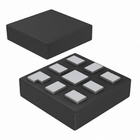
74AUP1G885GM,125 NXP Semiconductors, 74AUP1G885GM,125 Datasheet - Page 11

74AUP1G885GM,125
Manufacturer Part Number
74AUP1G885GM,125
Description
IC GATE DUAL FUNCTION 8-XQFN
Manufacturer
NXP Semiconductors
Series
74AUPr
Datasheet
1.74AUP1G885GM125.pdf
(23 pages)
Specifications of 74AUP1G885GM,125
Number Of Circuits
1
Package / Case
8-XQFN
Logic Type
Configurable Multiple Function
Number Of Inputs
3
Schmitt Trigger Input
Yes
Output Type
Single-Ended
Current - Output High, Low
4mA, 4mA
Voltage - Supply
0.8 V ~ 3.6 V
Operating Temperature
-40°C ~ 125°C
Mounting Type
Surface Mount
Product
MUX Gates
Logic Family
74AUP
High Level Output Current
- 4 mA
Low Level Output Current
4 mA
Propagation Delay Time
17.3 ns
Supply Voltage (max)
3.6 V
Supply Voltage (min)
0.8 V
Maximum Operating Temperature
+ 125 C
Mounting Style
SMD/SMT
Minimum Operating Temperature
- 40 C
Operating Temperature Range
- 40 C to + 125 C
Output Current
20 mA
Output Voltage
3.6 V
Power Dissipation
250 mW
Lead Free Status / RoHS Status
Lead free / RoHS Compliant
Lead Free Status / RoHS Status
Lead free / RoHS Compliant, Lead free / RoHS Compliant
Other names
568-4388-2
74AUP1G885GM-G
74AUP1G885GM-G
935280766125
74AUP1G885GM-G
74AUP1G885GM-G
935280766125
NXP Semiconductors
Table 8.
Voltages are referenced to GND (ground = 0 V; for test circuit see
[1]
[2]
[3]
[4]
12. Waveforms
Table 9.
74AUP1G885
Product data sheet
Symbol Parameter
C
C
Supply voltage
V
0.8 V to 3.6 V
Fig 6.
CC
L
PD
= 5 pF, 10 pF, 15 pF and 30 pF
All typical values are measured at nominal V
t
All specified values are the average typical values over all stated loads.
C
P
f
f
C
V
N = number of inputs switching;
Σ(C
pd
i
o
D
CC
PD
= input frequency in MHz;
L
= output frequency in MHz;
is the same as t
= output load capacitance in pF;
= C
L
is used to determine the dynamic power dissipation (P
= supply voltage in V;
× V
power dissipation
capacitance
Measurement points are given in
Logic levels: V
The data input (A, B, C) to output (nY) propagation delays
PD
Dynamic characteristics
Measurement points
CC
× V
2
× f
CC
o
2
) = sum of the outputs.
× f
PLH
i
× N + Σ(C
OL
and t
and V
PHL
Output
V
0.5 × V
Conditions
f
A, B, C input
i
OH
L
M
= 1 MHz; V
.
V
V
V
V
V
V
× V
nY output
are typical output voltage levels that occur with the output load.
CC
CC
CC
CC
CC
CC
CC
= 0.8 V
= 1.1 V to 1.3 V
= 1.4 V to 1.6 V
= 1.65 V to 1.95 V
= 2.3 V to 2.7 V
= 3.0 V to 3.6 V
CC
2
…continued
× f
Table
GND
o
V
V
All information provided in this document is subject to legal disclaimers.
) where:
OH
I
OL
CC
V
= GND to V
I
9.
.
Rev. 6 — 21 October 2010
Input
V
0.5 × V
M
CC
V
D
M
in μW).
CC
V
[3][4]
M
t
PHL
Figure
Min
-
-
-
-
-
-
7.
Typ
25 °C
2.7
2.9
3.0
3.1
3.5
4.1
V
V
[1]
I
CC
Max
t
PLH
-
-
-
-
-
-
001aae356
Low-power dual function gate
Min
74AUP1G885
-
-
-
-
-
-
−40 °C to +125 °C
(85 °C)
Max
t
≤ 3.0 ns
r
-
-
-
-
-
-
= t
© NXP B.V. 2010. All rights reserved.
f
(125 °C)
Max
-
-
-
-
-
-
11 of 23
Unit
pF
pF
pF
pF
pF
pF


