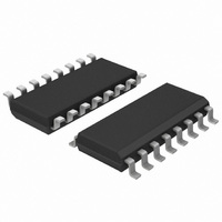
74HC4049D,653 NXP Semiconductors, 74HC4049D,653 Datasheet - Page 5

74HC4049D,653
Manufacturer Part Number
74HC4049D,653
Description
IC HEX INV LEVEL SHIFTER 16SOIC
Manufacturer
NXP Semiconductors
Series
74HCr
Datasheet
1.74HC4049DB112.pdf
(15 pages)
Specifications of 74HC4049D,653
Logic Type
Inverter
Number Of Inputs
1
Number Of Circuits
6
Current - Output High, Low
5.2mA, 5.2mA
Voltage - Supply
2 V ~ 6 V
Mounting Type
Surface Mount
Package / Case
16-SOIC (3.9mm Width)
Logic Family
HC
Number Of Channels Per Chip
6
Polarity
Inverting
Supply Voltage (max)
6 V
Supply Voltage (min)
2 V
Maximum Operating Temperature
+ 125 C
Mounting Style
SMD/SMT
High Level Output Current
- 5.2 mA
Low Level Output Current
5.2 mA
Minimum Operating Temperature
- 40 C
Number Of Lines (input / Output)
6 / 6
Propagation Delay Time
85 ns at 2 V, 17 ns at 4.5 V, 14 ns at 6 V
Lead Free Status / RoHS Status
Lead free / RoHS Compliant
Operating Temperature
-
Lead Free Status / Rohs Status
Details
Other names
74HC4049D-T
74HC4049D-T
933714800653
74HC4049D-T
933714800653
NXP Semiconductors
Table 6.
At recommended operating conditions; voltages are referenced to GND (ground = 0 V).
10. Dynamic characteristics
Table 7.
Voltages are referenced to GND (ground = 0 V); C
[1]
[2]
[3]
74HC4049
Product data sheet
Symbol Parameter
V
I
I
C
Symbol Parameter
t
t
C
I
CC
pd
t
OL
I
PD
t
t
C
P
f
f
C
V
pd
t
i
o
D
CC
PD
= input frequency in MHz;
L
is the same as t
= output frequency in MHz;
is the same as t
= output load capacitance in pF;
= C
is used to determine the dynamic power dissipation (P
= supply voltage in V;
LOW-level
output voltage
input leakage
current
supply current
input
capacitance
propagation
delay
transition
time
power
dissipation
capacitance
PD
Static characteristics
Dynamic characteristics
V
CC
2
f
THL
PLH
i
N + (C
and t
Conditions
nA to nY; see
Yn; see
C
V
and t
I
L
V
V
V
V
V
V
V
= GND to V
Conditions
V
V
V
V
V
V
= 50 pF; f = 1 MHz;
TLH
CC
CC
CC
CC
CC
CC
CC
I
I
CC
I
I
CC
PHL
I
I
I
I
I
= V
= V
= 15 V; V
= 15 V or GND; I
O
O
O
O
O
.
= 2.0 V
= 4.5 V
= 5 V; C
= 6.0 V
= 2.0 V
= 4.5 V
= 6.0 V
L
= 6.0 V
= 6.0 V
= 20 A; V
= 20 A; V
= 20 A; V
= 4.0 mA; V
= 5.2 mA; V
.
Figure 7
V
IH
CC
…continued
or V
CC
or GND;
2
Figure 7
CC
CC
L
IL
f
= 15 pF
o
= 6.0 V
All information provided in this document is subject to legal disclaimers.
CC
CC
CC
) where:
CC
CC
= 2.0 V
= 4.5 V
= 6.0 V
O
= 4.5 V
= 6.0 V
= 0 A;
Rev. 3 — 30 December 2010
L
= 50 pF unless otherwise specified; for test circuit see
[1]
[2]
[3]
D
Min
in W).
Min
-
-
-
-
-
-
-
-
-
-
-
-
-
-
-
-
-
T
T
amb
amb
Typ
Typ
= 25 C
3.5
28
10
19
14
= 25 C
8
8
7
6
-
-
-
-
-
-
-
-
Max
Max
0.26
0.26
0.1
0.5
0.1
0.1
0.1
2.0
85
17
14
75
15
13
-
-
-
Hex inverting HIGH-to-LOW level shifter
T
Min
T
amb
Min
amb
-
-
-
-
-
-
-
-
to +85 C
-
-
-
-
-
-
-
-
-
+85 C
= 40 C to
= 40 C
Max
105
Max
0.33
0.33
1.0
5.0
21
18
95
19
16
0.1
0.1
0.1
20
-
-
-
T
Min
amb
Min
T
74HC4049
-
-
-
-
-
-
-
-
-
-
-
amb
-
-
-
-
-
-
to +125 C
+125 C
© NXP B.V. 2010. All rights reserved.
= 40 C to
= 40 C
Figure
Max
1.0
5.0
Max
130
110
0.1
0.1
0.1
0.4
0.4
40
26
22
22
19
-
-
-
8.
Unit
V
V
V
V
V
A
A
A
pF
5 of 15
Unit
ns
ns
ns
ns
ns
ns
ns
pF


