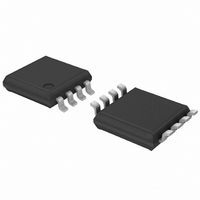
74HC3G14DP,125 NXP Semiconductors, 74HC3G14DP,125 Datasheet - Page 5

74HC3G14DP,125
Manufacturer Part Number
74HC3G14DP,125
Description
IC INV SCHMITT-TRIGGER 8-TSSOP
Manufacturer
NXP Semiconductors
Series
74HCr
Datasheet
1.74HCT3G14DP125.pdf
(18 pages)
Specifications of 74HC3G14DP,125
Number Of Circuits
3
Logic Type
Inverter with Schmitt Trigger
Package / Case
8-TSSOP
Number Of Inputs
1
Current - Output High, Low
5.2mA, 5.2mA
Voltage - Supply
2 V ~ 6 V
Operating Temperature
-40°C ~ 125°C
Mounting Type
Surface Mount
Logic Family
74HC
High Level Output Current
- 5.2 mA
Low Level Output Current
5.2 mA
Propagation Delay Time
125 ns, 25 ns, 21 ns
Supply Voltage (max)
6 V
Supply Voltage (min)
2 V
Maximum Operating Temperature
+ 125 C
Minimum Operating Temperature
- 40 C
Mounting Style
SMD/SMT
Operating Supply Voltage
5 V
Lead Free Status / RoHS Status
Lead free / RoHS Compliant
Lead Free Status / RoHS Status
Lead free / RoHS Compliant, Lead free / RoHS Compliant
Other names
74HC3G14DP-G
74HC3G14DP-G
935272126125
74HC3G14DP-G
935272126125
Available stocks
Company
Part Number
Manufacturer
Quantity
Price
Part Number:
74HC3G14DP,125
Manufacturer:
NXP/恩智浦
Quantity:
20 000
NXP Semiconductors
Table 7.
Voltages are referenced to GND (ground = 0 V). All typical values are measured at T
Table 8.
Voltages are referenced to GND (ground = 0 V); for test circuit see
74HC_HCT3G14_3
Product data sheet
Symbol Parameter
I
C
Symbol Parameter
74HC3G14
V
V
V
74HCT3G14
V
V
V
CC
I
T+
T
H
T+
T
H
I
CC
supply current per input pin; V
additional
supply current
input
capacitance
positive-going
threshold voltage
negative-going
threshold voltage
hysteresis voltage
positive-going
threshold voltage
negative-going
threshold voltage
hysteresis voltage
Static characteristics
Transfer characteristics
Conditions
V
per input;
V
V
I
CC
I
= V
= V
= 4.5 V to 5.5 V;
CC
CC
Conditions
see
see
(V
Figure 7
see
see
(V
Figure 7
or GND; I
…continued
V
V
V
V
V
V
T+
V
V
V
V
V
V
V
T+
V
V
CC
CC
CC
CC
CC
CC
CC
CC
CC
CC
CC
CC
CC
CC
CC
2.1 V; I
Figure
Figure
Figure
Figure
= 2.0 V
= 4.5 V
= 6.0 V
= 2.0 V
= 4.5 V
= 6.0 V
V
= 2.0 V
= 4.5 V
= 6.0 V
= 4.5 V
= 5.5 V
= 4.5 V
= 5.5 V
V
= 4.5 V
= 5.5 V
CC
T
T
and
and
); see
); see
O
= 5.5 V;
6,
6,
6,
6,
O
= 0 A
Figure 9
Figure 8
= 0 A;
Figure 7
Figure 7
Figure 7
Figure 7
Figure
Figure
Rev. 03 — 8 May 2009
6,
6,
Min
-
-
-
25 C
Typ
2.0
Figure
-
-
74HC3G14; 74HCT3G14
1.00
2.30
3.00
0.30
1.13
1.50
0.30
0.60
0.80
1.20
1.40
0.50
0.60
0.40
0.40
Min
Max
300
1.0
11.
-
25 C
1.18
2.60
3.46
0.60
1.47
2.06
0.60
1.13
1.40
1.58
1.78
0.87
1.11
0.71
0.67
Typ
40 C to +85 C
Min
-
-
-
Max
1.50
3.15
4.20
0.90
2.00
2.60
1.00
1.40
1.70
1.90
2.10
1.20
1.40
amb
-
-
Triple inverting Schmitt trigger
= 25 C.
Max
375
10
1.00
2.30
3.00
0.30
1.13
1.50
0.30
0.60
0.80
1.20
1.40
0.50
0.60
0.40
0.40
Min
-
40 C to +125 C
(85 C)
40 C to +125 C Unit
Min
Max
1.50
3.15
4.20
0.90
2.00
2.60
1.00
1.40
1.70
1.90
2.10
1.20
1.40
-
-
-
-
-
© NXP B.V. 2009. All rights reserved.
(125 C)
Max
410
Max
1.50
3.15
4.20
0.90
2.00
2.60
1.00
1.40
1.70
1.90
2.10
1.20
1.40
20
-
-
-
5 of 18
Unit
V
V
V
V
V
V
V
V
V
V
V
V
V
V
V
pF
A
A


