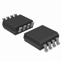
74AHCT3G14DC,125 NXP Semiconductors, 74AHCT3G14DC,125 Datasheet - Page 7

74AHCT3G14DC,125
Manufacturer Part Number
74AHCT3G14DC,125
Description
IC INV SCHMITT TRIGGER 8VSSOP
Manufacturer
NXP Semiconductors
Series
74AHCTr
Datasheet
1.74AHCT3G14DC125.pdf
(18 pages)
Specifications of 74AHCT3G14DC,125
Number Of Circuits
3
Logic Type
Inverter with Schmitt Trigger
Package / Case
US8, 8-VSSOP
Number Of Inputs
1
Current - Output High, Low
8mA, 8mA
Voltage - Supply
4.5 V ~ 5.5 V
Operating Temperature
-40°C ~ 125°C
Mounting Type
Surface Mount
Logic Family
AHCT
High Level Output Current
- 8 mA
Low Level Output Current
8 mA
Supply Voltage (max)
5.5 V
Supply Voltage (min)
4.5 V
Maximum Operating Temperature
+ 125 C
Mounting Style
SMD/SMT
Operating Supply Voltage
5 V
Lead Free Status / RoHS Status
Lead free / RoHS Compliant
Lead Free Status / RoHS Status
Lead free / RoHS Compliant, Lead free / RoHS Compliant
Other names
74AHCT3G14DC-G
74AHCT3G14DC-G
935275104125
74AHCT3G14DC-G
935275104125
NXP Semiconductors
Table 9.
GND = 0 V; t
[1]
[2]
[3]
[4]
13. Waveforms
Table 10.
74AHC_AHCT3G14
Product data sheet
Symbol Parameter
74AHCT3G14
t
C
Type number
74AHC3G14
74AHCT3G14
pd
Fig 7.
PD
t
Typical values are measured at V
Typical values are measured at V
C
P
f
f
C
V
Σ(C
pd
i
o
D
CC
PD
= input frequency in MHz;
L
= output frequency in MHz;
is the same as t
= output load capacitance in pF;
= C
L
is used to determine the dynamic power dissipation P
= supply voltage in V;
Y output
× V
A input
propagation
delay
power
dissipation
capacitance
The test data is given in
The input (nA) to output (nY) propagation
delays
PD
Dynamic characteristics
Test data
CC
r
× V
= t
2
× f
CC
f
≤
o
2
) = sum of the outputs.
3.0 ns; for test circuit see
× f
PLH
i
+ Σ (C
V
Conditions
nA to nY;
V
per buffer;
C
V
M
and t
V
CC
I
L
C
C
= GND to V
M
= 50 pF; f
L
L
L
t
PHL
= 4.5 V to 5.5 V
PHL
= 15 pF
= 50 pF
× V
Input
V
GND to V
GND to 3.0 V
.
Table 10
CC
I
CC
CC
2
× f
= 3.3 V.
= 5.0 V.
i
= 1 MHz;
…continued
CC
o
) where:
CC
All information provided in this document is subject to legal disclaimers.
Figure
t
PLH
mna033
Rev. 6 — 18 November 2010
8.
[1]
[3]
[4]
D
(μW).
Min
-
-
-
74AHC3G14; 74AHCT3G14
V
0.5 × V
1.5 V
Fig 8.
25 °C
M
Typ
4.1
5.9
12
CC
GENERATOR
Max
7.0
8.5
Test data is given in
Definitions for test circuit:
C
R
impedance Z
Test circuit for measuring switching times
-
PULSE
L
T
= Load capacitance.
= Termination resistance should be equal to output
−40 °C to +85 °C −40 °C to +125 °C Unit
Min
1.0
1.0
-
o
of the pulse generator.
V
I
Triple inverting Schmitt trigger
Max
10.0
8.0
Table
-
R T
Output
V
0.5 × V
0.5 × V
M
DUT
V
10.
CC
Min
1.0
1.0
CC
CC
-
V
© NXP B.V. 2010. All rights reserved.
O
Max
11.0
9.0
C L
mna101
-
7 of 18
ns
ns
pF


