74AUP2GU04GM,115 NXP Semiconductors, 74AUP2GU04GM,115 Datasheet - Page 2
74AUP2GU04GM,115
Manufacturer Part Number
74AUP2GU04GM,115
Description
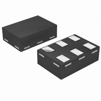
IC INVERTER DUAL 1-INPUT 6XSON
Manufacturer
NXP Semiconductors
Series
74AUPr
Datasheet
1.74AUP2GU04GM115.pdf
(19 pages)
Specifications of 74AUP2GU04GM,115
Number Of Circuits
2
Logic Type
Inverter
Package / Case
6-XSON (Micropak™), SOT-886
Number Of Inputs
1
Current - Output High, Low
4mA, 4mA
Voltage - Supply
0.8 V ~ 3.6 V
Operating Temperature
-40°C ~ 125°C
Mounting Type
Surface Mount
Logic Family
AUP
High Level Output Current
- 4 mA
Low Level Output Current
4 mA
Supply Voltage (max)
3.6 V
Supply Voltage (min)
0.8 V
Maximum Operating Temperature
+ 125 C
Mounting Style
SMD/SMT
Operating Supply Voltage
1.8 V, 2.5 V, 3.3 V
Lead Free Status / RoHS Status
Lead free / RoHS Compliant
Lead Free Status / RoHS Status
Lead free / RoHS Compliant, Lead free / RoHS Compliant
Other names
568-2582-2
935280001115
935280001115


NXP Semiconductors
4. Marking
Table 2.
[1]
5. Functional diagram
6. Pinning information
74AUP2GU04
Product data sheet
Type number
74AUP2GU04GW
74AUP2GU04GM
74AUP2GU04GF
74AUP2GU04GN
74AUP2GU04GS
Fig 1.
Fig 4.
The pin 1 indicator is located on the lower left corner of the device, below the marking code.
GND
1A
2A
1
3
Logic symbol
Pin configuration SOT363
Marking
1
2
3
1A
2A
74AUP2GU04
6.1 Pinning
001aad699
mnb106
1Y
2Y
6
5
4
6
4
1Y
V
2Y
CC
All information provided in this document is subject to legal disclaimers.
Fig 2.
Fig 5.
Rev. 3 — 10 November 2010
GND
IEC logic symbol
Pin configuration SOT886
1
3
1A
2A
Transparent top view
74AUP2GU04
1
2
3
1
1
mnb107
Marking code
aD
aD
aD
aD
aD
001aad700
6
5
4
1Y
V
2Y
6
4
CC
[1]
Low-power dual unbuffered inverter
Fig 3.
Fig 6.
A
GND
74AUP2GU04
540 Ω
Logic diagram (one gate)
Pin configuration SOT891,
SOT1115 and SOT1202
1A
2A
Transparent top view
74AUP2GU04
1
2
3
© NXP B.V. 2010. All rights reserved.
V
CC
001aad701
6
5
4
50 Ω
1Y
V
2Y
CC
001aad073
2 of 19
Y
Related parts for 74AUP2GU04GM,115
Image
Part Number
Description
Manufacturer
Datasheet
Request
R

Part Number:
Description:
74aup2gu04 Low-power Dual Unbuffered Inverter
Manufacturer:
NXP Semiconductors
Datasheet:
Part Number:
Description:
NXP Semiconductors designed the LPC2420/2460 microcontroller around a 16-bit/32-bitARM7TDMI-S CPU core with real-time debug interfaces that include both JTAG andembedded trace
Manufacturer:
NXP Semiconductors
Datasheet:

Part Number:
Description:
NXP Semiconductors designed the LPC2458 microcontroller around a 16-bit/32-bitARM7TDMI-S CPU core with real-time debug interfaces that include both JTAG andembedded trace
Manufacturer:
NXP Semiconductors
Datasheet:
Part Number:
Description:
NXP Semiconductors designed the LPC2468 microcontroller around a 16-bit/32-bitARM7TDMI-S CPU core with real-time debug interfaces that include both JTAG andembedded trace
Manufacturer:
NXP Semiconductors
Datasheet:
Part Number:
Description:
NXP Semiconductors designed the LPC2470 microcontroller, powered by theARM7TDMI-S core, to be a highly integrated microcontroller for a wide range ofapplications that require advanced communications and high quality graphic displays
Manufacturer:
NXP Semiconductors
Datasheet:
Part Number:
Description:
NXP Semiconductors designed the LPC2478 microcontroller, powered by theARM7TDMI-S core, to be a highly integrated microcontroller for a wide range ofapplications that require advanced communications and high quality graphic displays
Manufacturer:
NXP Semiconductors
Datasheet:
Part Number:
Description:
The Philips Semiconductors XA (eXtended Architecture) family of 16-bit single-chip microcontrollers is powerful enough to easily handle the requirements of high performance embedded applications, yet inexpensive enough to compete in the market for hi
Manufacturer:
NXP Semiconductors
Datasheet:
Part Number:
Description:
The XA-S3 device is a member of Philips Semiconductors? XA(eXtended Architecture) family of high performance 16-bitsingle-chip microcontrollers
Manufacturer:
NXP Semiconductors
Datasheet:

Part Number:
Description:
The NXP BlueStreak LH75401/LH75411 family consists of two low-cost 16/32-bit System-on-Chip (SoC) devices
Manufacturer:
NXP Semiconductors
Datasheet:
Part Number:
Description:
The NXP LPC3130/3131 combine an 180 MHz ARM926EJ-S CPU core, high-speed USB2
Manufacturer:
NXP Semiconductors
Datasheet:
Part Number:
Description:
The NXP LPC3141 combine a 270 MHz ARM926EJ-S CPU core, High-speed USB 2
Manufacturer:
NXP Semiconductors
Part Number:
Description:
The NXP LPC3143 combine a 270 MHz ARM926EJ-S CPU core, High-speed USB 2
Manufacturer:
NXP Semiconductors

Part Number:
Description:
The NXP LPC3152 combines an 180 MHz ARM926EJ-S CPU core, High-speed USB 2
Manufacturer:
NXP Semiconductors
Part Number:
Description:
The NXP LPC3154 combines an 180 MHz ARM926EJ-S CPU core, High-speed USB 2
Manufacturer:
NXP Semiconductors