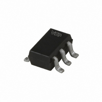
74LVC2G14GW,125 NXP Semiconductors, 74LVC2G14GW,125 Datasheet - Page 3

74LVC2G14GW,125
Manufacturer Part Number
74LVC2G14GW,125
Description
IC SCHMITT-TRIG SGL INV SC88-6
Manufacturer
NXP Semiconductors
Series
74LVCr
Datasheet
1.74LVC2G14GW125.pdf
(20 pages)
Specifications of 74LVC2G14GW,125
Number Of Circuits
2
Logic Type
Inverter with Schmitt Trigger
Package / Case
SC-70-6, SC-88, SOT-363
Number Of Inputs
1
Current - Output High, Low
32mA, 32mA
Voltage - Supply
1.65 V ~ 5.5 V
Operating Temperature
-40°C ~ 125°C
Mounting Type
Surface Mount
Logic Family
LVC
High Level Output Current
- 32 mA
Low Level Output Current
32 mA
Supply Voltage (max)
5.5 V
Supply Voltage (min)
1.65 V
Maximum Operating Temperature
+ 125 C
Mounting Style
SMD/SMT
Operating Supply Voltage
1.8 V, 2.5 V, 3.3 V, 5 V
Logical Function
Inverter Schmit Trig
Number Of Elements
2
Input Type
Schmitt Trigger
Propagation Delay Time
12ns
Operating Supply Voltage (typ)
1.8/2.5/3.3/5V
Package Type
SOT-363
Operating Temp Range
-40C to 125C
Pin Count
6
Quiescent Current
40uA
Output Type
Schmitt Trigger
Technology
CMOS
Mounting
Surface Mount
Operating Temperature Classification
Automotive
Operating Supply Voltage (max)
5.5V
Operating Supply Voltage (min)
1.65V
Lead Free Status / RoHS Status
Lead free / RoHS Compliant
Lead Free Status / RoHS Status
Lead free / RoHS Compliant, Lead free / RoHS Compliant
Other names
568-4840-2
74LVC2G14GW,125
74LVC2G14GW-G
74LVC2G14GW-G
935273895125
74LVC2G14GW,125
74LVC2G14GW-G
74LVC2G14GW-G
935273895125
Available stocks
Company
Part Number
Manufacturer
Quantity
Price
Company:
Part Number:
74LVC2G14GW,125
Manufacturer:
NXP Semiconductors
Quantity:
2 350
NXP Semiconductors
7. Pinning information
Table 3.
8. Functional description
Table 4.
[1]
74LVC2G14
Product data sheet
Symbol
1A
GND
2A
2Y
V
1Y
Input
nA
L
H
Fig 4. Pin configuration SOT363
CC
H = HIGH voltage level;
L = LOW voltage level.
GND
1A
2A
and SOT457
Pin description
Function table
1
2
3
74LVC2G14
7.1 Pinning
7.2 Pin description
001aab672
[1]
6
5
4
1Y
V
2Y
CC
Pin
1
2
3
4
5
6
All information provided in this document is subject to legal disclaimers.
Fig 5. Pin configuration SOT886
Rev. 5 — 29 October 2010
GND
1A
2A
Transparent top view
74LVC2G14
1
2
3
Dual inverting Schmitt trigger with 5 V tolerant input
Output
nY
H
L
001aab673
6
5
4
1Y
V
2Y
CC
Description
data input
ground (0 V)
data input
data output
supply voltage
data input
Fig 6. Pin configuration SOT891,
GND
SOT1115 and SOT1202
1A
2A
Transparent top view
74LVC2G14
74LVC2G14
1
2
3
© NXP B.V. 2010. All rights reserved.
001aaf957
6
5
4
1Y
V
2Y
CC
3 of 20


