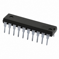
74ABT377AN,112 NXP Semiconductors, 74ABT377AN,112 Datasheet - Page 4

74ABT377AN,112
Manufacturer Part Number
74ABT377AN,112
Description
IC OCTAL D F-F W/ENABLE 20DIP
Manufacturer
NXP Semiconductors
Series
74ABTr
Type
D-Type Busr
Datasheet
1.74ABT377ADB118.pdf
(12 pages)
Specifications of 74ABT377AN,112
Function
Standard
Output Type
Non-Inverted
Number Of Elements
1
Number Of Bits Per Element
8
Frequency - Clock
250MHz
Delay Time - Propagation
3.1ns
Trigger Type
Positive Edge
Current - Output High, Low
32mA, 64mA
Voltage - Supply
4.5 V ~ 5.5 V
Operating Temperature
-40°C ~ 85°C
Mounting Type
Through Hole
Package / Case
20-DIP (0.300", 7.62mm)
Lead Free Status / RoHS Status
Lead free / RoHS Compliant
Other names
74ABT377AN
74ABT377AN
935244050112
74ABT377AN
935244050112
Philips Semiconductors
FUNCTION TABLE
H = High voltage level
h = High voltage level one set-up time prior to the Low-to-High clock transition
L = Low voltage level
l
X = Don’t care
ABSOLUTE MAXIMUM RATINGS
NOTES:
1. Stresses beyond those listed may cause permanent damage to the device. These are stress ratings only and functional operation of the
2. The performance capability of a high-performance integrated circuit in conjunction with its thermal environment can create junction
3. The input and output voltage ratings may be exceeded if the input and output current ratings are observed.
RECOMMENDED OPERATING CONDITIONS
1997 Feb 26
SYMBOL
SYMBOL
Octal D-type flip-flop with enable
= Low voltage level one set-up time prior to the Low-to-High clock transition
= Low-to-High clock transition
device at these or any other conditions beyond those indicated under “recommended operating conditions” is not implied. Exposure to
absolute-maximum-rated conditions for extended periods may affect device reliability.
temperatures which are detrimental to reliability. The maximum junction temperature of this integrated circuit should not exceed 150 C.
V
T
I
V
V
T
I
OUT
V
I
V
I
t/ v
amb
I
OK
OUT
OH
V
V
OL
stg
CC
IK
CC
IH
IL
I
I
E
H
h
l
l
DC supply voltage
DC input diode current
DC input voltage
DC output diode current
DC output voltage
DC output current
Storage temperature range
DC supply voltage
Input voltage
High-level input voltage
Low-level input voltage
High-level output current
Low-level output current
Input transition rise or fall rate
Operating free-air temperature range
PARAMETER
3
INPUTS
3
CP
X
1, 2
PARAMETER
Dn
X
X
h
l
output in Off or High state
4
output in Low state
CONDITIONS
OUTPUTS
no change
no change
V
V
O
I
Qn
< 0
H
< 0
L
MIN
–40
4.5
2.0
0
0
Load “1”
Load “0”
Hold (do nothing)
LIMITS
OPERATING MODE
–0.5 to +7.0
–1.2 to +7.0
–0.5 to +5.5
–65 to 150
RATING
–18
–50
128
MAX
V
–32
+85
74ABT377A
5.5
0.8
64
5
CC
Product specification
UNIT
UNIT
ns/V
mA
mA
mA
mA
mA
V
V
V
V
V
V
V
C
C


