74ABT377AN,112 NXP Semiconductors, 74ABT377AN,112 Datasheet - Page 2
74ABT377AN,112
Manufacturer Part Number
74ABT377AN,112
Description
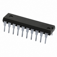
IC OCTAL D F-F W/ENABLE 20DIP
Manufacturer
NXP Semiconductors
Series
74ABTr
Type
D-Type Busr
Datasheet
1.74ABT377ADB118.pdf
(12 pages)
Specifications of 74ABT377AN,112
Function
Standard
Output Type
Non-Inverted
Number Of Elements
1
Number Of Bits Per Element
8
Frequency - Clock
250MHz
Delay Time - Propagation
3.1ns
Trigger Type
Positive Edge
Current - Output High, Low
32mA, 64mA
Voltage - Supply
4.5 V ~ 5.5 V
Operating Temperature
-40°C ~ 85°C
Mounting Type
Through Hole
Package / Case
20-DIP (0.300", 7.62mm)
Lead Free Status / RoHS Status
Lead free / RoHS Compliant
Other names
74ABT377AN
74ABT377AN
935244050112
74ABT377AN
935244050112


Philips Semiconductors
FEATURES
QUICK REFERENCE DATA
ORDERING INFORMATION
PIN CONFIGURATION
20-Pin Plastic DIP
20-Pin plastic SO
20-Pin Plastic SSOP Type II
20-Pin Plastic TSSOP Type I
1997 Feb 26
Ideal for addressable register applications
8-bit positive edge-triggered register
Enable for address and data synchronization applications
Output capability: +64mA/-32mA
Latch-up protection exceeds 500mA per Jedec JC40.2 Std 17
ESD protection exceeds 2000V per MIL STD 883 Method 3015
and 200V per Machine Model
Power-up reset
Octal D-type flip-flop with enable
SYMBOL
I
t
t
C
CCH
PLH
PHL
IN
PACKAGES
GND
Q0
Q1
Q2
Q3
D0
D1
D2
D3
E
Propagation delay
CP to Qn
Input capacitance
Total current supply
10
1
2
3
4
5
6
7
8
9
PARAMETER
TEMPERATURE RANGE
20
19
18
17
16
15
14
13
12
11
V
Q7
D7
D6
Q6
Q5
D5
D4
Q4
CP
–40 C to +85 C
–40 C to +85 C
–40 C to +85 C
–40 C to +85 C
CC
SA00155
OUTSIDE NORTH AMERICA
2
Outputs High; V
74ABT377A PW
74ABT377A DB
DESCRIPTION
The 74ABT377A high-performance BiCMOS device combines low
static and dynamic power dissipation with high speed and high
output drive.
The 74ABT377A has 8 edge-triggered D-type flip-flops with
individual D inputs and Q outputs. The common buffered clock (CP)
input loads all flip-flops simultaneously when the Enable (E) input is
Low.
The register is fully edge triggered. The state of each D input, one
set-up time before the Low-to-High clock transition, is transferred to
the corresponding flip-flop’s Q output.
The E input must be stable one setup time prior to the Low-to-High
clock transition for predictable operation.
LOGIC SYMBOL
T
74ABT377A N
74ABT377A D
amb
C
L
V
= 50pF; V
CONDITIONS
= 25 C; GND = 0V
I
= 0V or V
11
1
CC
CC
CC
Q0 Q1 Q2
D0 D1 D2 D3
CP
OE
= 5V
3
2
= 5.5V
4
5
74ABT377PWA DH
NORTH AMERICA
7
6
74ABT377A DB
74ABT377A N
74ABT377A D
Q3
8
9
Q4 Q5 Q6
D4 D5 D6 D7
12
13
14
15
TYPICAL
16
17
74ABT377A
500
3.1
3.6
4
Product specification
Q7
18
19
DWG NUMBER
853-1457 17800
SOT146-1
SOT163-1
SOT339-1
SOT360-1
UNIT
SA00152
pF
nA
ns
Related parts for 74ABT377AN,112
Image
Part Number
Description
Manufacturer
Datasheet
Request
R

Part Number:
Description:
NXP Semiconductors designed the LPC2420/2460 microcontroller around a 16-bit/32-bitARM7TDMI-S CPU core with real-time debug interfaces that include both JTAG andembedded trace
Manufacturer:
NXP Semiconductors
Datasheet:

Part Number:
Description:
NXP Semiconductors designed the LPC2458 microcontroller around a 16-bit/32-bitARM7TDMI-S CPU core with real-time debug interfaces that include both JTAG andembedded trace
Manufacturer:
NXP Semiconductors
Datasheet:
Part Number:
Description:
NXP Semiconductors designed the LPC2468 microcontroller around a 16-bit/32-bitARM7TDMI-S CPU core with real-time debug interfaces that include both JTAG andembedded trace
Manufacturer:
NXP Semiconductors
Datasheet:
Part Number:
Description:
NXP Semiconductors designed the LPC2470 microcontroller, powered by theARM7TDMI-S core, to be a highly integrated microcontroller for a wide range ofapplications that require advanced communications and high quality graphic displays
Manufacturer:
NXP Semiconductors
Datasheet:
Part Number:
Description:
NXP Semiconductors designed the LPC2478 microcontroller, powered by theARM7TDMI-S core, to be a highly integrated microcontroller for a wide range ofapplications that require advanced communications and high quality graphic displays
Manufacturer:
NXP Semiconductors
Datasheet:
Part Number:
Description:
The Philips Semiconductors XA (eXtended Architecture) family of 16-bit single-chip microcontrollers is powerful enough to easily handle the requirements of high performance embedded applications, yet inexpensive enough to compete in the market for hi
Manufacturer:
NXP Semiconductors
Datasheet:
Part Number:
Description:
The XA-S3 device is a member of Philips Semiconductors? XA(eXtended Architecture) family of high performance 16-bitsingle-chip microcontrollers
Manufacturer:
NXP Semiconductors
Datasheet:

Part Number:
Description:
The NXP BlueStreak LH75401/LH75411 family consists of two low-cost 16/32-bit System-on-Chip (SoC) devices
Manufacturer:
NXP Semiconductors
Datasheet:
Part Number:
Description:
The NXP LPC3130/3131 combine an 180 MHz ARM926EJ-S CPU core, high-speed USB2
Manufacturer:
NXP Semiconductors
Datasheet:
Part Number:
Description:
The NXP LPC3141 combine a 270 MHz ARM926EJ-S CPU core, High-speed USB 2
Manufacturer:
NXP Semiconductors
Part Number:
Description:
The NXP LPC3143 combine a 270 MHz ARM926EJ-S CPU core, High-speed USB 2
Manufacturer:
NXP Semiconductors

Part Number:
Description:
The NXP LPC3152 combines an 180 MHz ARM926EJ-S CPU core, High-speed USB 2
Manufacturer:
NXP Semiconductors
Part Number:
Description:
The NXP LPC3154 combines an 180 MHz ARM926EJ-S CPU core, High-speed USB 2
Manufacturer:
NXP Semiconductors

Part Number:
Description:
Standard level N-channel enhancement mode Field-Effect Transistor (FET) in a plastic package using NXP High-Performance Automotive (HPA) TrenchMOS technology
Manufacturer:
NXP Semiconductors
Datasheet: