74ACT273MTCX Fairchild Semiconductor, 74ACT273MTCX Datasheet

IC FLIP FLOP OCT D TYPE 20TSSOP

74ACT273MTCX

Manufacturer Part Number
74ACT273MTCX
Description
IC FLIP FLOP OCT D TYPE 20TSSOP
Manufacturer
Fairchild Semiconductor
Series
74ACTr
Type
D-Type Busr
Datasheet

Specifications of 74ACT273MTCX

Function
Master Reset
Output Type
Non-Inverted
Number Of Elements
1
Number Of Bits Per Element
8
Frequency - Clock
189MHz
Delay Time - Propagation
6.5ns
Trigger Type
Positive Edge
Current - Output High, Low
24mA, 24mA
Voltage - Supply
4.5 V ~ 5.5 V
Operating Temperature
-40°C ~ 85°C
Mounting Type
Surface Mount
Package / Case
20-TSSOP
Dc
2006+
Lead Free Status / RoHS Status
Lead free / RoHS Compliant
© 2000 Fairchild Semiconductor Corporation
74AC273SC
74AC273SJ
74AC273MTC
74AC273PC
74ACT273SC
74ACT273SJ
74ACT273MTC
74ACT273PC
74AC273 • 74ACT273
Octal D-Type Flip-Flop
General Description
The AC273 and ACT273 have eight edge-triggered D-type
flip-flops with individual D-type inputs and Q outputs. The
common buffered Clock (CP) and Master Reset (MR) input
load and reset (clear) all flip-flops simultaneously.
The register is fully edge-triggered. The state of each D-
type input, one setup time before the LOW-to-HIGH clock
transition, is transferred to the corresponding flip-flop’s Q
output.
All outputs will be forced LOW independently of Clock or
Data inputs by a LOW voltage level on the MR input. The
device is useful for applications where the true output only
is required and the Clock and Master Reset are common to
all storage elements.
Ordering Code:
Device also available in Tape and Reel. Specify by appending suffix letter “X” to the ordering code.
Logic Symbols
FACT
Order Number
is a trademark of Fairchild Semiconductor Corporation.
Package Number
MTC20
MTC20
IEEE/IEC
M20B
M20D
M20B
M20D
N20A
N20A
20-Lead Small Outline Integrated Circuit (SOIC), JEDEC MS-013, 0.300 Wide
20-Lead Small Outline Package (SOP), EIAJ TYPE II, 5.3mm Wide
20-Lead Thin Shrink Small Outline Package (TSSOP), JEDEC MO-153, 4.4mm Wide
20-Lead Plastic Dual-In-Line Package (PDIP), JEDEC MS-001, 0.300 Wide
20-Lead Small Outline Integrated Circuit (SOIC), JEDEC MS-013, 0.300 Wide
20-Lead Small Outline Package (SOP), EIAJ TYPE II, 5.3mm Wide
20-Lead Thin Shrink Small Outline Package (TSSOP), JEDEC MO-153, 4.4mm Wide
20-Lead Plastic Dual-In-Line Package (PDIP), JEDEC MS-001, 0.300 Wide
DS009954
Features
Connection Diagram
Ideal buffer for microprocessor or memory
Eight edge-triggered D-type flip-flops
Buffered common clock
Buffered, asynchronous master reset
See 377 for clock enable version
See 373 for transparent latch version
See 374 for 3-STATE version
Outputs source/sink 24 mA
74ACT273 has TTL-compatible inputs
Package Description
November 1988
Revised August 2000
www.fairchildsemi.com

Related parts for 74ACT273MTCX

74ACT273MTCX Summary of contents

Page 1

... Plastic Dual-In-Line Package (PDIP), JEDEC MS-001, 0.300 Wide Device also available in Tape and Reel. Specify by appending suffix letter “X” to the ordering code. Logic Symbols IEEE/IEC FACT is a trademark of Fairchild Semiconductor Corporation. © 2000 Fairchild Semiconductor Corporation Features Ideal buffer for microprocessor or memory Eight edge-triggered D-type flip-flops ...

Page 2

Pin Descriptions Pin Names Description D –D Data Inputs Master Reset CP Clock Pulse Input Q –Q Data Outputs 0 7 Logic Diagram Please note that this diagram is provided only for the understanding of logic operations ...

Page 3

Absolute Maximum Ratings Supply Voltage ( Input Diode Current ( 0. 0. Input Voltage ( Output Diode Current ( ...

Page 4

AC Electrical Characteristics for AC Symbol Parameter f Maximum Clock MAX Frequency t Propagation Delay PLH Clock to Output t Propagation Delay PHL Clock to Output t Propagation Delay PHL MR to Output Note 5: Voltage Range 3.3 is 3.3V ...

Page 5

DC Electrical Characteristics for ACT V Symbol Parameter V Minimum HIGH Level 4.5 IH Input Voltage 5.5 V Maximum LOW Level 4.5 IL Input Voltage 5.5 V Minimum HIGH Level 4.5 OH Output Voltage 5.5 4.5 5.5 V Maximum LOW ...

Page 6

AC Operating Requirements for ACT Symbol Parameter t Setup Time, HIGH or LOW Hold Time, HIGH or LOW Clock Pulse Width W HIGH or LOW t MR Pulse ...

Page 7

Physical Dimensions inches (millimeters) unless otherwise noted 20-Lead Small Outline Integrated Circuit (SOIC), JEDEC MS-013, 0.300 Wide Package Number M20B 7 www.fairchildsemi.com ...

Page 8

Physical Dimensions inches (millimeters) unless otherwise noted (Continued) 20-Lead Small Outline Package (SOP), EIAJ TYPE II, 5.3mm Wide www.fairchildsemi.com Package Number M20D 8 ...

Page 9

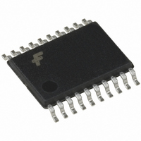
Physical Dimensions inches (millimeters) unless otherwise noted (Continued) 20-Lead Thin Shrink Small Outline Package (TSSOP), JEDEC MO-153, 4.4mm Wide Package Number MTC20 9 www.fairchildsemi.com ...

Page 10

Physical Dimensions inches (millimeters) unless otherwise noted (Continued) 20-Lead Plastic Dual-In-Line Package (PDIP), JEDEC MS-001, 0.300 Wide Fairchild does not assume any responsibility for use of any circuitry described, no circuit patent licenses are implied and Fairchild reserves the right ...

Related keywords