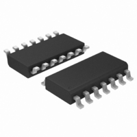
MC74ACT125DR2G ON Semiconductor, MC74ACT125DR2G Datasheet

MC74ACT125DR2G
Specifications of MC74ACT125DR2G
MC74ACT125DR2GOS
MC74ACT125DR2GOSTR
Available stocks
Related parts for MC74ACT125DR2G
MC74ACT125DR2G Summary of contents
Page 1
MC74AC125, MC74ACT125 Quad Buffer with 3−State Outputs Features • Outputs Source/Sink • ′ACT125 Has TTL Compatible Inputs • Pb−Free Packages are Available ...
Page 2
MAXIMUM RATINGS Symbol V DC Supply Voltage (Referenced to GND Input Voltage (Referenced to GND Output Voltage (Referenced to GND) out I DC Input Current, per Pin Output Sink/Source Current, per ...
Page 3
DC CHARACTERISTICS Symbol Parameter V Minimum High Level IH Input Voltage V Maximum Low Level IL Input Voltage V Minimum High Level OH Output Voltage V Minimum Low Level OL Output Voltage I Maximum Input IN Leakage Current V (OE) ...
Page 4
DC CHARACTERISTICS Symbol Parameter V Minimum High Level IH Input Voltage V Maximum Low Level IL Input Voltage Minimum High Level V OH Output Voltage V Minimum Low Level OL Output Voltage Maximum Input I IN Leakage Current I V ...
Page 5
... MC74AC125DR2 MC74AC125DR2G MC74AC125DTR2 MC74AC125DTR2G MC74AC125M MC74AC125MG MC74AC125MEL MC74AC125MELG MC74ACT125DR2 MC74ACT125DR2G MC74ACT125DTR2 MC74ACT125DTR2G MC74ACT125MEL MC74ACT125MELG MC74ACT125N MC74ACT125NG †For information on tape and reel specifications, including part orientation and tape sizes, please refer to our Tape and Reel Packaging Specifications Brochure, BRD8011/D. *This package is inherently Pb−Free. ...
Page 6
−T− SEATING PLANE 0.13 (0.005) PACKAGE DIMENSIONS PDIP−14 CASE 646−06 ISSUE http://onsemi.com 6 NOTES: 1. DIMENSIONING AND TOLERANCING PER ANSI ...
Page 7
... G −T− SEATING 14 PL PLANE 0.25 (0.010 14X 0.58 *For additional information on our Pb−Free strategy and soldering details, please download the ON Semiconductor Soldering and Mounting Techniques Reference Manual, SOLDERRM/D. PACKAGE DIMENSIONS SOIC−14 CASE 751A−03 ISSUE 0.25 (0.010 ...
Page 8
... S A −V− C 0.10 (0.004) −T− SEATING G D PLANE 14X 0.36 *For additional information on our Pb−Free strategy and soldering details, please download the ON Semiconductor Soldering and Mounting Techniques Reference Manual, SOLDERRM/D. PACKAGE DIMENSIONS TSSOP−14 CASE 948G−01 ISSUE 0.25 (0.010) ...
Page 9
... Opportunity/Affirmative Action Employer. This literature is subject to all applicable copyright laws and is not for resale in any manner. PUBLICATION ORDERING INFORMATION LITERATURE FULFILLMENT: Literature Distribution Center for ON Semiconductor P.O. Box 5163, Denver, Colorado 80217 USA Phone: 303−675−2175 or 800−344−3860 Toll Free USA/Canada Fax: 303− ...


