CY7C4261V-15JXC Cypress Semiconductor Corp, CY7C4261V-15JXC Datasheet
CY7C4261V-15JXC
Specifications of CY7C4261V-15JXC
Available stocks


Related parts for CY7C4261V-15JXC


CY7C4261V-15JXC Summary of contents
Page 1
... Features 3.3 V operation for low-power consumption and easy ■ integration into low-voltage systems High-speed, low-power, first-in first-out (FIFO) memories ■ × 9 (CY7C4261V) ■ × 9 (CY7C4271V) ■ × 9 (CY7C4281V) ■ 128 K × 9 (CY7C4291V) ■ 0.35-micron CMOS for optimum speed or power ■ High-speed 100-MHz operation (10-ns read/write cycle ■ ...
Page 2
... Document #: 38-06013 Rev 0–8 Input Register WEN1 WEN2/LD Write Dual Port RAM Array 16 K/32 K Write 64 K/128 Pointer Reset Logic Tristate Output Register OE Q 0–8 RCLK CY7C4261V/CY7C4271V CY7C4281V/CY7C4291V Flag Program Register EF PAE Flag Logic PAF FF Read Pointer Read Control REN1 REN2 Page [+] Feedback ...
Page 3
... Switching Waveforms .................................................... 11 Write Cycle Timing .................................................... 11 Read Cycle Timing .................................................... 11 Reset Timing .............................................................. 12 First Data Word Latency after Reset with Read and Write 13 Document #: 38-06013 Rev. *F CY7C4261V/CY7C4271V CY7C4281V/CY7C4291V Full Flag Timing ......................................................... 15 Programmable Almost Empty Flag Timing ................ 15 Programmable Almost Full Flag Timing .................... 16 Write Programmable Registers ................................. 16 Read Programmable Registers ...
Page 4
... Resets device to empty condition. A reset is required before an initial read or write operation after power-up. I When OE is LOW, the FIFO’s data outputs drive the bus to which they are connected HIGH, the FIFO’s outputs are in High Z (high-impedance) state. CY7C4261V/CY7C4271V CY7C4281V/CY7C4291V Page [+] Feedback ...
Page 5
... Empty Offset (LSB) Reg. Default Value = 007h 8 7 (MSB) Default Value = 000h 8 7 Full Offset (LSB) Reg Default Value = 007h 8 7 (MSB) Default Value = 000h CY7C4261V/CY7C4271V CY7C4281V/CY7C4291V shows the registers sizes and default Empty Offset (LSB) Reg. Default Value = 007h (MSB) ...
Page 6
... LOW-to-HIGH transition of WCLK by one flip-flop and is set LOW when the number of unread words in the FIFO is greater than or equal to CY7C4261V (16k – m), CY7C4271V (32k – m), CY7C4281V (64k – m) and CY7C4291V (128k – m). PAF is set HIGH by the LOW-to-HIGH transition of WCLK when the number of available memory locations is greater than m ...
Page 7
... REN1 and REN2 synchronized to RCLK, i.e exclusively updated by each rising edge of RCLK. Used in a Width-Expansion Configuration Reset (RS) 9 CY7C4261V CY7C4271V CY7C4281V CY7C4291V Read Enable 2 (REN2) CY7C4261V/CY7C4271V CY7C4281V/CY7C4291V Read Clock (RCLK) Read Enable 1 (REN1) Output Enable (OE) Programmable (PAE) Empty Flag (EF) #1 Empty Flag (EF Data Out (Q) ...
Page 8
... Ind – – Com’l – 4 Ind – – Test Conditions MHz, 3 CY7C4261V/CY7C4271V CY7C4281V/CY7C4291V [4] Ambient Temperature V CC 3.3 V 300 mV 0 °C to +70 °C 40 °C to +85 °C 3.3 V 300 mV 7C4261/71/81/91V- 7C4261/71/81/91V Min Max Min Max 2.4 – 2.4 – ...
Page 9
... Z0 = 50 Notes for all AC parameters except for t L OHZ for OHZ Document #: 38-06013 Rev. *F [8, 9] 3.0 V R2=510 GND 2 CC/2 3.0V GND CY7C4261V/CY7C4271V CY7C4281V/CY7C4291V All Input Pulses 90% 90% 10% 10% All Input Pulses 90% 90% 10% 10% Page [+] Feedback ...
Page 10
... CY7C4261V/CY7C4271V CY7C4281V/CY7C4291V 7C4261/71/81/91V Unit Max Min Max 66.7 – 40 MHz – 25 – ns – 10 – ns – 10 – ns – 6 – ns – 1 – ns – 6 – ns – ...
Page 11
... WFF t CKL t CLKL NO OPERATION t REF t REF t A Valid Data [13] SKEW1 , then FF may not change state until the next WCLK rising edge. SKEW1 , then EF may not change state until the next RCLK rising edge. SKEW2 CY7C4261V/CY7C4271V CY7C4281V/CY7C4291V No Operation No Operation t OHZ Page [+] Feedback ...
Page 12
... Holding WEN2/LD HIGH during reset will make the pin act as a second enable pin. Holding WEN2/LD LOW during reset will make the pin act as a load enable for the programmable flag offset registers. Document #: 38-06013 Rev RSR RSS t t RSR RSS t t RSR RSS t RSF t RSF t RSF CY7C4261V/CY7C4271V CY7C4281V/CY7C4291V [15 OE=0 Page [+] Feedback ...
Page 13
... The Latency Timing applies only at the Empty Boundary (EF = LOW). SKEW1 18. The first word is available the cycle after EF goes HIGH, always. Document #: 38-06013 Rev [17] t FRL t REF OLZ When t < minimum specification, t CLK SKEW2 SKEW1 CY7C4261V/CY7C4271V CY7C4281V/CY7C4291V [18 (maximum) = either 2 FRL CLK SKEW1 CLK Page [+] Feedback ...
Page 14
... The Latency Timing applies only at the Empty Boundary (EF = LOW). SKEW1 Document #: 38-06013 Rev Data Write 2 t ENS t ENS t t REF REF When t < minimum specification, t CLK SKEW2 SKEW1 CY7C4261V/CY7C4271V CY7C4281V/CY7C4291V t ENH t ENH [19] t FRL t t REF SKEW1 Data Read (maximum) = either 2 FRL CLK SKEW1 CLK Page ...
Page 15
... WFF t ENS Data Read t CLKL t ENH 22 t ENH WORDS t PAE t ENS , then FF may not change state until the next WCLK rising edge. SKEW1 CY7C4261V/CY7C4271V CY7C4281V/CY7C4291V No Write Data Write t WFF t ENH t A Next Data Read 23 IN FIFO t PAE t t ENS ENH Page ...
Page 16
... If a write is performed on this rising edge of the write clock, there will be Full (m1) words of the FIFO when PAF goes LOW. 25. PAF offset = m. 26 m words for CY7C4261V – m words for CY7C4271V m words for CY7C4281V, and 128 K m words for CY4291V. 27 the minimum time between a rising RCLK edge and a rising WCLK edge for PAF to change during that clock cycle ...
Page 17
... Switching Waveforms (continued) Read Programmable Registers t CLK t CLKH RCLK t ENS WEN2/LD t ENS REN1, REN2 Q – Document #: 38-06013 Rev CLKL t ENH t A Unknown PAE Offset LSB PAE Offset MSB CY7C4261V/CY7C4271V CY7C4281V/CY7C4291V PAF Offset MSB PAF Offset LSB Page [+] Feedback ...
Page 18
... Ordering Information Speed (ns) Ordering Code 10 CY7C4261V-10JXC 15 CY7C4261V-15JXC 10 CY7C4271V-10JXC 10 CY7C4281V-10JXC 10 CY7C4291V-10JXC 15 CY7C4291V-15JXC Ordering Code Definition 42xx Document #: 38-06013 Rev × 9 Low-Voltage Deep Sync FIFO Package Name Package Type J65 32-pin Pb-free plastic leaded chip carrier J65 32-pin Pb-free plastic leaded chip carrier 32 K × ...
Page 19
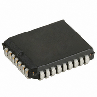
... Package Diagram Figure 3. 32-Pin Pb-free Plastic Leaded Chip Carrier J65, 51-85002 Document #: 38-06013 Rev. *F CY7C4261V/CY7C4271V CY7C4281V/CY7C4291V 51-85002 *C Page [+] Feedback ...
Page 20
... CE chip enable I/O input/output OE output enable SRAM static random access memory TSOP thin small outline package WE write enable Document #: 38-06013 Rev. *F CY7C4261V/CY7C4271V CY7C4281V/CY7C4291V Document Conventions Units of Measure Table 4. Units of Measure Symbol Unit of Measure ns nano seconds V volts µA micro amperes mA ...
Page 21
... SKEW1 Fixed flag timing diagram in Switching Waveforms section Added Pb-Free logo to top of front page Added CY7C4291V-15JXC, CY7C91V-10JXC, CY7C4281V-10JXC, CY7C4271V-10JXC, CY7C4261V-10JXC, CY7C4261V-15JXC to ordering infor- mation. Removed inactive parts from Ordering information and updated package diagram. Removed inactive part from Ordering Information table. ...
Page 22
... Deep Sync is a trademark of Cypress Semiconductor. All product and company names mentioned in this document are the trademarks of their respective holders. All products and company names mentioned in this document may be the trademarks of their respective holders. cypress.com/go/plc Revised March 30, 2011 CY7C4261V/CY7C4271V CY7C4281V/CY7C4291V PSoC Solutions psoc.cypress.com/solutions ...