CY7C4261-10JC Cypress Semiconductor Corp, CY7C4261-10JC Datasheet
CY7C4261-10JC
Specifications of CY7C4261-10JC


Related parts for CY7C4261-10JC


CY7C4261-10JC Summary of contents
Page 1
... FIFO on each WCLK cycle. The output port is controlled in a similar manner by a free-running read clock (RCLK) and two read enable pins (REN1, REN2). In addition, the CY7C4261/71 has an output enable pin (OE). The read (RCLK) and write (WCLK) clocks may be tied together for single-clock operation or the two clocks may be run independently for asynchronous read/write applications ...
Page 2
... Functional Description (continued) The CY7C4261/71 provides four status pins: Empty, Full, Programmable Almost Empty, and Programmable Almost Full. The Almost Empty/Almost Full flags are programmable to single word granularity. The programmable flags default to Empty+7 and Full–7. The flags are synchronous, i.e., they change state relative to either the read clock (RCLK) or the write clock (WCLK) ...
Page 3
... Density 16K × 9 Package 32-pin PLCC,TQFP Architecture The CY7C4261/71 consists of an array of 16K to 32K words of nine bits each (implemented by a dual-port array of SRAM cells), a read pointer, a write pointer, control signals (RCLK, WCLK, REN1, REN2, WEN1, WEN2, RS), and flags (EF, PAE, PAF, FF). ...
Page 4
... FF). The partial status flags (PAE and PAF) can be detected from any one device. Figure 2 demonstrates a 18-bit word width by using two CY7C4261/71s. Any word width can be attained by adding additional CY7C4261/71s. When the CY7C4261/ Width-Expansion Configu- ration, the Read Enable (REN2) control input can be grounded (see Figure 2) ...
Page 5
... Figure 2. Block Diagram of 16K × 18/32K × 18 Deep Sync FIFO Memory Used in a Width-Expansion Configuration Document #: 38-06015 Rev. *B RESET (RS) 9 CY7C4261/ Read Enable 2 (REN2) CY7C4261 CY7C4271 READ CLOCK (RCLK) READ ENABLE 1 (REN1) OUTPUT ENABLE (OE) PROGRAMMABLE(PAE) EMPTY FLAG (EF) #1 EMPTY FLAG (EF DATA OUT (Q) ...
Page 6
... V < Com’l 35 Ind/Mil 40 Com’l 10 Ind/Mil 15 Description Test Conditions MHz 5.0V CC [10, 11] 3.0V GND R2 680 1.91V . OHZ CY7C4261 CY7C4271 Ambient Temperature + +125 C Min. Max. Min. Max. Min. 2.4 2.4 2.4 0.4 0.4 2.0 V 2 2.2 V 2.2 V 2.2 ...
Page 7
... Notes: 12. Pulse widths less than minimum values are not allowed. 13. Values guaranteed by design, not currently tested. Document #: 38-06015 Rev. *B 7C4261/71 10 7C4261/71 15 7C4261/71 25 7C4261/71 35 Min. Max. Min. 100 4 [13 [13 CY7C4261 CY7C4271 Max. Min. Max. Min. Max. 66.7 40 28.6 MHz ...
Page 8
... CLKL t ENH NO OPERATION t REF [15] t SKEW1 , then FF may not change state until the next WCLK rising edge. SKEW1 , then EF may not change state until the next RCLK rising edge. SKEW2 CY7C4261 CY7C4271 ENH NO OPERATION NO OPERATION t WFF t REF VALID DATA t OHZ Page ...
Page 9
... The first word is available the cycle after EF goes HIGH, always. Document #: 38-06015 Rev RSS t RSS t RSS t RSF t RSF t RSF D 1 [19] t FRL t SKEW1 t REF t OLZ t OE (maximum When t < minimum specification, t CLK SKEW2 SKEW2 CY7C4261 CY7C4271 t RSR t RSR t RSR [17 OE [20 (maximum) = either 2 FRL CLK SKEW1 Page ...
Page 10
... REN2 LOW OE Q –Q DATA IN OUTPUT REGISTER 0 8 Document #: 38-06015 Rev. *B [19 REF REF DATA WRITE t WFF t ENH t A DATA READ CY7C4261 CY7C4271 t DS DATA WRITE 2 t ENH t ENS t t ENH ENS [19] t FRL t t SKEW1 DATA READ NO WRITE [14] t SKEW1 t t ...
Page 11
... If a write is performed on this rising edge of the write clock, there will be Full 25. PAF offset = m. 26. 16,384 m words for CY7C4261, 32,768 27 the minimum time between a rising RCLK edge and a rising WCLK edge for PAF to change during that clock cycle. If the time between the rising edge of RCLK and ...
Page 12
... WEN2/LD t ENS REN1, REN2 Q – Document #: 38-06015 Rev CLKL t ENH PAE OFFSET PAE OFFSET LSB MSB t CLKL t ENH t A UNKNOWN PAE OFFSET LSB CY7C4261 CY7C4271 PAF OFFSET PAF OFFSET LSB MSB PAF OFFSET MSB PAF OFFSET PAE OFFSET MSB LSB Page ...
Page 13
... V =3.0V IN 0. MHz 0.60 4.00 4.50 5.00 5.50 SUPPLY VOLTAGE (V) Ordering Information 16Kx9 Deep Sync FIFO Speed (ns) Ordering Code 10 CY7C4261-10AC CY7C4261-10JC CY7C4261-10AI CY7C4261-10JI 15 CY7C4261-15AC CY7C4261-15JC CY7C4261-15AI CY7C4261-15JI 25 CY7C4261-25AC CY7C4261-25JC CY7C4261-25AI CY7C4261-25JI Document #: 38-06015 Rev. *B vs. SUPPLY A 1.60 1.40 1.20 1.00 T =25 C ...
Page 14
... J65 32-Lead Plastic Leaded Chip Carrier A32 32-Lead Thin Quad Flatpack J65 32-Lead Plastic Leaded Chip Carrier A32 32-Lead Thin Quad Flatpack J65 32-Lead Plastic Leaded Chip Carrier Subgroups CY7C4261 CY7C4271 Package Operating Type Range Commercial Industrial Package Operating Type Range ...
Page 15
... REF t 9, 10, 11 RFF t 9, 10, 11 WEF t 9, 10, 11 WFF t 9, 10, 11 WHF t 9, 10, 11 RHF t 9, 10, 11 RAE t 9, 10, 11 RPE t 9, 10, 11 WAF t 9, 10, 11 WPF t 9, 10, 11 XOL t 9, 10, 11 XOH Document #: 38-06015 Rev. *B Subgroups CY7C4261 CY7C4271 Page ...
Page 16
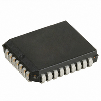
... Package Diagrams 32-Lead Thin Plastic Quad Flatpack 7 × 7 × 1.0 mm A32 Document #: 38-06015 Rev. *B 32-Lead Plastic Leaded Chip Carrier J65 CY7C4261 CY7C4271 51-85063-*B 51-85002-*B Page ...
Page 17
... Package Diagrams (continued) All product and company names mentioned in this document are the trademarks of their respective holders. Document #: 38-06015 Rev. *B 32-Pin Rectangular Leadless Chip Carrier L55 MIL-STD-1835 C-12 CY7C4261 CY7C4271 51-80068-** Page ...
Page 18
... Document History Page Document Title: CY7C4261, CY7C4271 16K/32K X 9 Deep Synchronous FIFOs Document Number: 38-06015 REV. ECN NO. Issue Date ** 106476 09/10/01 *A 122267 12/26/02 *B 127853 08/22/03 Document #: 38-06015 Rev. *B Orig. of Change SZV Changed from Spec number: 38-00658 to 38-06015 RBI Added power-up requirements Maximum Ratings Information ...