74F899QC Fairchild Semiconductor, 74F899QC Datasheet
74F899QC
Specifications of 74F899QC
Available stocks


Related parts for 74F899QC


74F899QC Summary of contents
Page 1
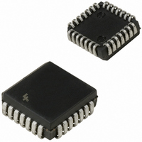
... Package Number 74F899SC M28B 28-Lead Small Outline Integrated Circuit (SOIC), JEDEC MS-013, 0.300 Wide 74F899QC V28A 28-Lead Plastic Lead Chip Carrier (PLCC), JEDEC MO-047, 0.450 Square Devices also available in Tape and Reel. Specify by appending the suffix letter “X” to the ordering code. ...
Page 2
Input Loading/Fan-Out Pin Names A –A Data Inputs Data Outputs B –B Data Inputs Data Outputs APAR A Bus Parity Input/Output BPAR B Bus Parity Input/Output Parity Select Input ODD/EVEN Output Enable Inputs GBA, GAB Mode ...
Page 3
Function Table Inputs GAB GBA SEL LEA LEB Busses A and B are 3-STATE Generates parity from B[0:7] based on O/E (Note 1). Generated parity Generated parity checked against BPAR ...
Page 4
Absolute Maximum Ratings Storage Temperature Ambient Temperature under Bias Junction Temperature under Bias V Pin Potential to Ground Pin CC Input Voltage (Note 3) Input Current (Note 3) Voltage Applied to Output in HIGH State (with V 0V) CC Standard ...
Page 5
DC Electrical Characteristics Symbol Parameter Min I Output Leakage IL I Current OZL I Output Short-Circuit Current OS I Bus Drainage Test ZZ I Power Supply Current CCH I Power Supply Current CCL I Power Supply Current CCZ AC Electrical ...
Page 6
AC Path A , APAR B , BPAR BPAR A , APAR BPAR n (B APAR ERRA n (B ERRB) n www.fairchildsemi.com FIGURE 1. FIGURE 2. FIGURE 3. 6 ...
Page 7
AC Path (Continued) O/E ERRA O/E ERRB O/E BPAR (O/E APAR) APAR ERRA (BPAR ERRB) FIGURE 4. FIGURE 5. FIGURE 6. 7 www.fairchildsemi.com ...
Page 8
AC Path (Continued) ZH, HZ ZL, LZ www.fairchildsemi.com FIGURE 7. FIGURE 8. FIGURE 9. 8 ...
Page 9
AC Path (Continued) SEL BPAR (SEL APAR) LEA BPAR, B[0:7] (LEB APAR, A[0:7]) TS(H), TH(H) LEA APAR, A[0:7] (LEB BPAR, B[0:7]) FIGURE 10. FIGURE 11. FIGURE 12. 9 www.fairchildsemi.com ...
Page 10
AC Path (Continued) TS(L), TH(L) LEA APAR, A[0:7] (LEB BPAR, B[0:7]) www.fairchildsemi.com FIGURE 13. FIGURE 14. 10 ...
Page 11
Physical Dimensions inches (millimeters) unless otherwise noted 28-Lead Small Outline Integrated Circuit (SOIC), JEDEC MS-013, 0.300 Wide Package Number M28B 11 www.fairchildsemi.com ...
Page 12
Physical Dimensions inches (millimeters) unless otherwise noted (Continued) 28-Lead Plastic Lead Chip Carrier (PLCC), JEDEC MO-047, 0.450 Square Fairchild does not assume any responsibility for use of any circuitry described, no circuit patent licenses are implied and Fairchild reserves the ...